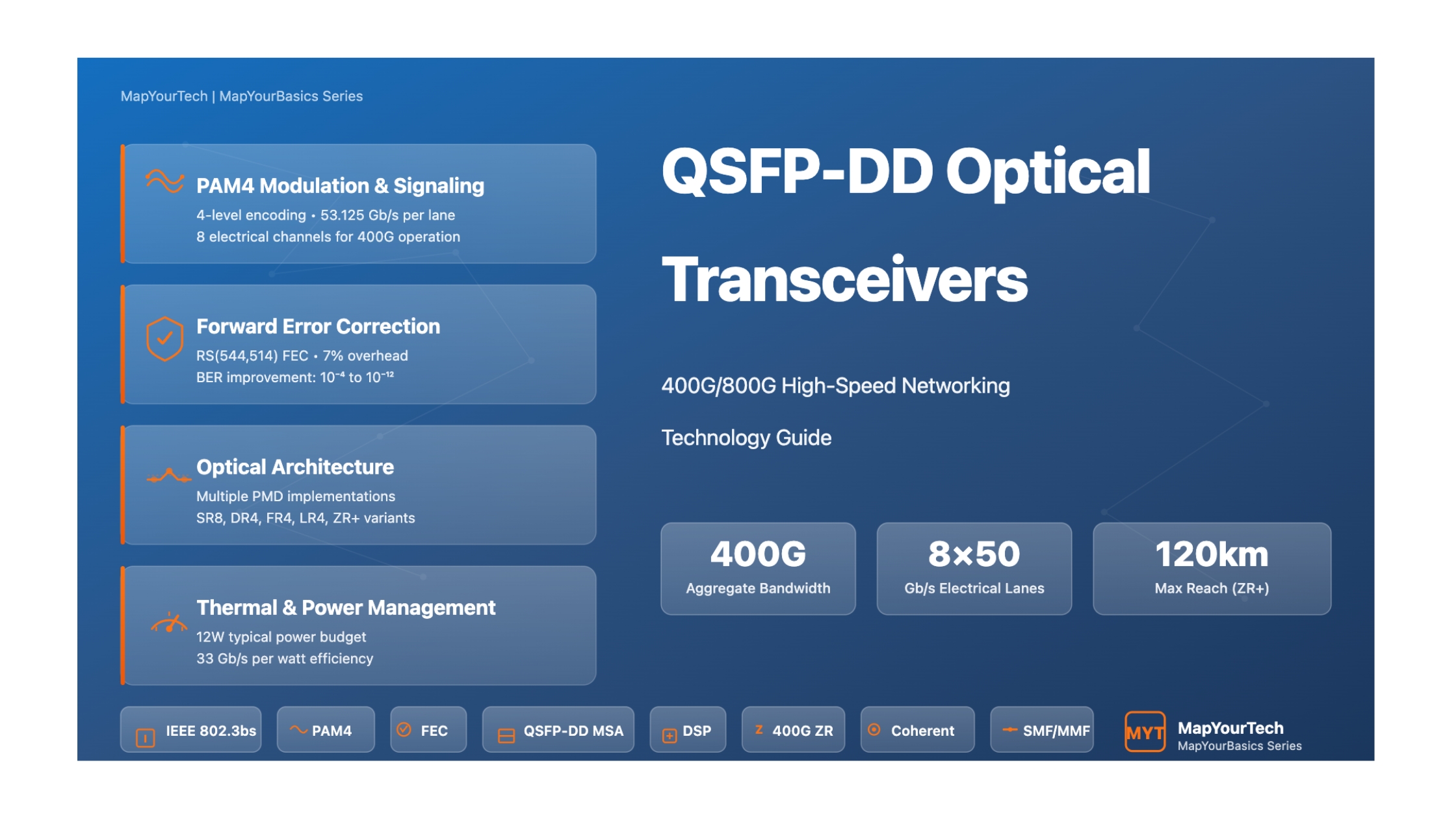

QSFP-DD: Quad Small Form-Factor Pluggable Double Density Optical Transceivers
A Comprehensive Technical Guide to 400G/800G High-Speed Optical Networking Technology
Introduction
QSFP-DD (Quad Small Form-Factor Pluggable Double Density) represents a transformative advancement in optical transceiver technology, addressing the exponential growth in data center bandwidth requirements and the demands of modern high-performance computing environments. As data traffic continues to surge driven by cloud computing, artificial intelligence, machine learning, and 5G networks, the need for higher-capacity, energy-efficient optical interconnects has become paramount.
Market Context: The global 400G optical transceiver market is experiencing remarkable growth, with projections indicating expansion from USD 1.35 billion in 2023 to an estimated USD 7.67 billion by 2032, reflecting a compound annual growth rate (CAGR) of 21.3%. The QSFP-DD form factor has emerged as the mainstream solution for 400G and 800G deployments, with China's cloud providers alone deploying over 1.5 million QSFP-DD/400G modules in 2024.
What is QSFP-DD?
QSFP-DD is an advanced hot-pluggable optical transceiver form factor that doubles the bandwidth density of traditional QSFP28 modules by implementing a double-density design with eight electrical lanes instead of four. This architecture enables aggregate data rates up to 400 Gb/s using 8 × 50 Gb/s electrical interfaces with PAM4 modulation, with a clear evolution path to 800 Gb/s using 8 × 100 Gb/s signaling.
Key Architectural Innovation
The QSFP-DD form factor achieves its performance through a sophisticated electrical interface design that maintains backward compatibility while dramatically increasing capacity. The module features 76 electrical contact pins arranged in a double-row configuration, compared to the 38-pin single-row design of QSFP28. This allows for eight high-speed differential pairs on both transmit and receive paths, doubling the data throughput while maintaining a similar physical footprint.
Why QSFP-DD is Important
The significance of QSFP-DD technology extends across multiple dimensions of modern networking infrastructure:
Bandwidth Scaling: QSFP-DD provides a clear path from 100G to 400G and beyond, enabling network operators to scale bandwidth capacity without requiring complete infrastructure overhauls. The technology supports various physical media dependent (PMD) implementations, from short-reach multimode fiber solutions to long-haul single-mode applications extending to 40 kilometers or more.
Port Density Optimization: By delivering 400G in the same port footprint traditionally used for 100G QSFP28 modules, QSFP-DD enables four times the bandwidth density in data center switches and routers. This translates to significant reductions in equipment costs, power consumption per bit, and data center floor space requirements.
Backward Compatibility: A critical advantage of QSFP-DD is its mechanical and electrical backward compatibility with QSFP28, QSFP56, and QSFP+ modules. This allows QSFP28 modules to be inserted into QSFP-DD ports, connecting to four of the eight electrical channels. This compatibility provides network operators with investment protection and enables gradual migration strategies.
Power Efficiency: Modern QSFP-DD modules implement advanced digital signal processing (DSP) and forward error correction (FEC) to achieve superior power efficiency. Typical 400G QSFP-DD modules consume 12W maximum power, delivering approximately 33 Gb/s per watt, compared to 100G QSFP28 modules at 25 Gb/s per watt.
Real-World Relevance
The deployment of QSFP-DD technology is transforming network architectures across multiple sectors. Hyperscale data centers operated by major cloud providers have adopted QSFP-DD as their standard for leaf-spine fabric interconnections, enabling AI cluster servers with 400Gb/s networking speeds. The NVIDIA DGX H100 GPU server system, for example, is equipped with four 400G ports, pushing leaf-spine fabric networking to high port densities of 800Gb/s.
Telecommunications operators are leveraging 400G QSFP-DD modules to build efficient backbone and metro networks, supporting 5G infrastructure and long-haul transmission. The IP-over-DWDM architecture using 400G ZR/ZR+ transceivers and passive Mux/DeMux filters can offer up to 75% cost savings compared to traditional muxponder systems for distances within 80 kilometers.
Industry Applications
| Application Sector | Use Case | Benefits |
|---|---|---|
| Data Center Interconnect | Cross-facility links, cloud backbone | High capacity, simplified architecture, cost reduction |
| Hyperscale Cloud | Leaf-spine fabrics, storage networks | Extreme port density, power efficiency, scalability |
| 5G Networks | Mobile backhaul, fronthaul aggregation | Low latency, high throughput, flexible deployment |
| Enterprise Networks | Core switching, campus backbone | Future-proof design, investment protection, compatibility |
| AI/ML Infrastructure | GPU interconnects, training clusters | Ultra-low latency, high bandwidth, job completion efficiency |
| Financial Services | High-frequency trading, risk analysis | Minimal jitter, reliable redundancy, high throughput |
What You'll Learn in This Guide
This comprehensive guide provides an in-depth exploration of QSFP-DD technology, structured to take you from foundational concepts to advanced implementation strategies:
- Historical Evolution: Understand the technology timeline from QSFP+ through QSFP28 to QSFP-DD, including key milestones, industry standards development, and the forces driving form factor evolution.
- Core Technical Principles: Master the fundamental concepts of PAM4 modulation, forward error correction, gearbox functionality, and the electrical-to-optical conversion processes that enable 400G/800G operation.
- System Architecture: Explore detailed breakdowns of transmitter and receiver paths, digital signal processor implementations, thermal management strategies, and management interface protocols.
- Mathematical Foundations: Examine the equations governing signal integrity, power budgets, dispersion penalties, and bit error rate calculations that determine link performance.
- Module Variants: Compare different QSFP-DD types including SR8, DR4, FR4, LR4, LR8, and ZR implementations, understanding their optimal use cases and tradeoffs.
- Practical Applications: Study real-world deployment scenarios, case studies from major deployments, troubleshooting methodologies, and best practices for implementation.
- Interactive Analysis: Utilize four sophisticated simulators to model link performance, compare module types, analyze power budgets, and optimize system configurations.
Key Concepts Preview
PAM4 Modulation
Four-level Pulse Amplitude Modulation (PAM4) is the cornerstone of QSFP-DD's bandwidth efficiency. Unlike traditional Non-Return-to-Zero (NRZ) encoding that uses two signal levels to represent binary data, PAM4 uses four distinct amplitude levels, enabling two bits to be transmitted per symbol. This effectively doubles the data rate without increasing the baud rate, though it introduces additional complexity in signal processing and requires sophisticated equalization and error correction.
Forward Error Correction (FEC)
FEC is essential for achieving reliable high-speed transmission in QSFP-DD modules. The most commonly implemented FEC scheme is Reed-Solomon RS(544,514), which can correct burst errors and random errors introduced by PAM4's reduced signal-to-noise ratio. FEC adds approximately 7% overhead but enables transmission over distances and through impairments that would otherwise be impossible, typically improving pre-FEC bit error rates from 2.4×10⁻⁴ to post-FEC rates better than 1×10⁻¹².
Gearbox Functionality
The gearbox within QSFP-DD modules performs critical rate adaptation between the host electrical interface and the optical interface. For a 400G DR4 module, the gearbox converts eight host lanes of 26.5625 GBd PAM4 (equivalent to 53.125 Gb/s per lane) into four optical lanes of 53.125 GBd PAM4 (equivalent to 106.25 Gb/s per lane). This rate conversion, combined with FEC encoding/decoding and retiming functions, ensures reliable data transmission across the electrical-optical boundary.
By the conclusion of this guide, you will possess a comprehensive understanding of QSFP-DD technology sufficient to make informed decisions about module selection, network design, deployment strategies, and troubleshooting approaches. Whether you are a network architect planning a data center upgrade, a system engineer integrating optical transceivers into equipment designs, or a technical professional seeking to deepen your knowledge of high-speed optical communications, this guide provides the technical depth and practical insights required for success in modern high-performance networking environments.
Historical Context & Evolution
The evolution of small form-factor pluggable transceivers represents one of the most significant technological progressions in optical networking history. Understanding this timeline provides crucial context for appreciating QSFP-DD's role in meeting contemporary bandwidth demands and anticipating future developments.
Technology Timeline
Early Beginnings: GBIC and SFP (1990s-2003)
The journey toward modern small form-factor transceivers began with the Gigabit Interface Converter (GBIC) in the late 1990s. While revolutionary for its time in enabling hot-pluggable Gigabit Ethernet and Fibre Channel connections, GBIC modules were relatively large and consumed significant board space. The Small Form-factor Pluggable (SFP) transceiver emerged in 2003 as a more compact solution, approximately half the size of GBIC, supporting data rates up to 4.25 Gb/s.
The Quad Era: QSFP+ (2006-2012)
The Quad Small Form-factor Pluggable (QSFP) specification was introduced in 2006 to address the growing demand for 40 Gigabit Ethernet. By aggregating four 10 Gb/s channels using NRZ modulation, QSFP+ modules achieved 40 Gb/s aggregate throughput in a compact, hot-pluggable format. The QSFP+ MSA (Multi-Source Agreement) specification provided standardization that enabled multi-vendor interoperability and rapid industry adoption.
SFF-8661 and SFF-8679 Standards
The Small Form Factor Committee developed critical specifications that defined QSFP+ mechanical, electrical, and management interfaces. SFF-8661 established the 4X pluggable module specifications, while SFF-8679 defined the electrical base specifications. These standards provided the foundation for all subsequent QSFP evolution, establishing pin-out configurations, power requirements, and thermal management approaches that persist in modern implementations.
100G Transition: QSFP28 (2013-2018)
QSFP28 emerged in 2013 as the industry's answer to 100 Gigabit Ethernet requirements. Maintaining the same mechanical form factor as QSFP+, QSFP28 increased the per-lane data rate from 10 Gb/s to 25 Gb/s using improved NRZ signaling, achieving 100 Gb/s aggregate bandwidth. This represented a critical inflection point where significant bandwidth increases were achieved through signaling rate improvements rather than channel count increases.
The IEEE 802.3bm standard, ratified in 2015, defined 100GBASE-SR4 for multimode fiber and 100GBASE-LR4 for single-mode fiber applications. QSFP28 adoption accelerated rapidly, with shipment volumes exceeding 100 million units by 2018. The form factor's success stemmed from its optimal balance of density, power consumption (typically 3.5W), and cost-effectiveness for data center leaf-spine architectures.
The 400G Challenge: Form Factor Wars (2017-2020)
As the industry contemplated 400 Gigabit Ethernet, multiple competing form factors emerged. The CFP8 (C Form-factor Pluggable 8) specification allowed very early 400G adopters to develop and validate implementations, but its large size made it unsuitable for high-density switching applications. Three primary form factors competed for 400G market leadership:
| Form Factor | Introduction | Key Advantages | Limitations | Market Outcome |
|---|---|---|---|---|
| CFP8 | 2016 | Early to market, proven technology | Very large size, limited density | Early adopter only, minimal volume |
| OSFP | 2017 | Superior thermal design, larger PCB area | No backward compatibility, new ecosystem | Strong in specialized applications |
| QSFP-DD | 2017 | Backward compatible, established ecosystem | Tighter thermal constraints | Dominant market leader for 400G |
Key Milestones and Breakthroughs
2017: QSFP-DD MSA Formation
The QSFP-DD Multi-Source Agreement group was established in 2017 with participation from major networking equipment manufacturers, optical component suppliers, and data center operators. The MSA's charter was to define a scalable, backward-compatible form factor for 400G and beyond. Initial specification releases focused on mechanical dimensions, electrical interface definitions, and thermal management requirements.
Breakthrough Achievement: The QSFP-DD design successfully maintained backward compatibility with QSFP28 modules while doubling the electrical channel count from four to eight. This was accomplished through innovative connector design featuring 76 electrical contacts in a double-row configuration, compared to QSFP28's 38-contact single-row design. The extended module "nose" (18.45mm maximum height compared to QSFP28's 8.5mm) provided additional internal volume for enhanced thermal management and more sophisticated integrated circuits.
2017: IEEE 802.3bs Standardization
The IEEE 802.3bs standard for 200 Gb/s and 400 Gb/s Ethernet was ratified in December 2017, providing the PHY layer specifications that QSFP-DD modules would implement. Critical specifications included 400GBASE-SR8 for short-reach multimode applications, 400GBASE-DR4 for 500m single-mode reach, and 400GBASE-FR4/LR4 for 2km and 10km applications respectively.
2018-2019: PAM4 Signaling Maturation
The adoption of PAM4 modulation represented a fundamental shift from NRZ signaling. Extensive research and development addressed PAM4's challenges including reduced signal-to-noise ratio, increased sensitivity to nonlinearities, and higher digital signal processing complexity. Industry collaboration through organizations like the OIF (Optical Internetworking Forum) established CEI-56G-PAM4 electrical interface specifications that enabled reliable 56 Gb/s per lane operation.
2020: Volume Production and Deployment
By 2020, QSFP-DD modules entered volume production with multiple vendors offering compliant solutions. Hyperscale data center operators began deploying 400G QSFP-DD modules in production networks, validating the technology's performance, reliability, and interoperability. Initial deployments focused on DR4 (500m single-mode) and SR8 (multimode) variants for data center interconnection.
2021-2022: Coherent Integration and Extended Reach
A significant breakthrough occurred with the integration of coherent optical technology into QSFP-DD and OSFP form factors. The 400ZR implementation, standardized by the OIF, enabled 400G transmission over 80-120km distances using sophisticated DSP-based coherent detection. This eliminated the need for external transponders in metro and regional network applications. The OpenZR+ MSA further extended capabilities to support enhanced performance and additional features beyond the base 400ZR specification.
Current State of Technology (2024-2025)
The QSFP-DD ecosystem has matured significantly, with widespread industry adoption and continuous innovation. Current developments include:
800G Evolution: QSFP-DD modules supporting 800 Gb/s aggregate bandwidth using 8 × 100 Gb/s electrical lanes have transitioned from development to production deployment. These modules leverage 100 GBd PAM4 signaling and advanced DSP implementations. In 2024, major suppliers shipped over 15 million 800G modules to support AI cluster deployments and hyperscale data center expansions.
Silicon Photonics Integration: The adoption of silicon photonics technology has improved QSFP-DD power efficiency and manufacturing scalability. Silicon photonics modules integrate optical components directly onto silicon substrates, reducing assembly complexity and enabling lower cost points. Production 400G silicon photonics modules achieve power consumption below 10W per port, compared to 12-16W for earlier discrete implementations.
Enhanced Thermal Management: Improved thermal designs enable higher performance within the QSFP-DD form factor constraints. Innovations include advanced heat sink geometries, thermal interface material optimization, and active cooling integration in high-power applications. These advances support both 800G operation and coherent implementations that historically required larger form factors.
Smart Module Features: Modern QSFP-DD modules incorporate embedded microcontrollers that monitor temperature, power, and bit error rate in real-time. Over 500,000 smart modules were shipped in 2024, enabling predictive failure alerts and improving uptime by approximately 15% compared to standard implementations. The Common Management Interface Specification (CMIS) 5.1 provides standardized access to these telemetry capabilities.
Market Dynamics (2024)
The Asia-Pacific region leads QSFP-DD deployment volume at 39% of global shipments, driven by massive cloud infrastructure buildouts in China, enterprise network upgrades in India, and short-reach module adoption in Japan and South Korea. China's cloud providers alone deployed over 1.5 million QSFP-DD/400G modules in 2024. North America maintains the largest share of coherent QSFP-DD deployments, with significant adoption of 400G ZR+ modules for metro and regional network applications.
Future Outlook
The trajectory of QSFP-DD technology points toward continued evolution in multiple dimensions:
1.6T and Beyond: Development efforts are underway for 1.6 Tb/s aggregate bandwidth using advanced modulation formats and higher baud rates. QSFP-DD800 specifications define mechanical and thermal requirements for these implementations, though widespread deployment is projected for 2026-2027.
Co-Packaged Optics (CPO): The industry is exploring co-packaged optics where optical transceivers are integrated directly with switch ASICs, eliminating electrical interconnect limitations. CPO integration kits debuted in 2024, with trial deployments achieving 32 ports with 1W per-port optical links and switch-to-switch latency below 0.1 microseconds. While CPO represents a paradigm shift, pluggable modules like QSFP-DD will continue serving applications requiring flexibility and field replaceability.
Linear Pluggable Optics (LPO): LPO eliminates retiming and DSP functions in short-reach applications, significantly reducing module power consumption. QSFP-DD LPO implementations consume approximately 5W per port, enabling greener top-of-rack switch deployments. Over 150,000 LPO units were shipped to enterprise and cloud operators in 2024, delivering 50% power reduction compared to standard QSFP28 modules.
Extended Temperature Ranges: To address deployment in industrial, outdoor, and harsh environment applications, extended and industrial temperature grade QSFP-DD modules are becoming available. These variants operate from -40°C to +85°C, compared to standard commercial ratings of 0°C to +70°C, enabling QSFP-DD adoption in telecommunications outside plant and industrial automation scenarios.
The evolution from GBIC to QSFP-DD represents five orders of magnitude in bandwidth increase over approximately 25 years, from 1 Gb/s to 400 Gb/s, with 800 Gb/s and 1.6 Tb/s implementations on the horizon. This remarkable progression reflects continuous innovation in modulation formats, semiconductor technology, optical component design, and system architecture. QSFP-DD has emerged as the dominant form factor for current-generation 400G deployments and is well-positioned to support the transition to 800G and beyond, ensuring its relevance for years to come.
Core Concepts & Fundamentals
Understanding QSFP-DD technology requires mastery of several fundamental concepts that underpin its operation. This section provides detailed explanations of the key principles, technical terminology, and operational mechanisms that enable 400G/800G transmission in the QSFP-DD form factor.
Basic Principles Explained
Parallel Optical Transmission Architecture
QSFP-DD employs a parallel transmission architecture where data is distributed across multiple independent optical channels. For a 400G implementation, the module converts eight electrical input lanes operating at 53.125 Gb/s each (using PAM4 modulation at 26.5625 GBd) into four optical lanes operating at 106.25 Gb/s each. This parallelization strategy offers several advantages over serial approaches, including reduced per-lane data rates (easing component specifications), improved power efficiency through parallel processing, and enhanced reliability through inherent redundancy.
Electrical-to-Optical Conversion Process
The conversion from electrical to optical signals involves multiple sophisticated processing stages. Incoming electrical signals first pass through equalization circuits that compensate for channel impairments. A retiming and reclocking stage removes accumulated jitter. The gearbox function then performs rate adaptation, converting the host interface data rate to match the optical interface requirements. Forward error correction encoding adds redundancy for error detection and correction. Finally, laser drivers modulate optical sources (typically EMLs or DMLs) to generate the transmitted optical signals.
Double-Density Connector Innovation
The "Double Density" designation in QSFP-DD refers to the innovative connector design that achieves twice the signal density of QSFP28. The QSFP-DD electrical connector features 76 contacts arranged in two rows, compared to QSFP28's 38 contacts in a single row. This double-stacking approach maintains similar overall connector dimensions while accommodating eight differential signal pairs for transmit (TX0-TX7) and eight for receive (RX0-RX7), along with necessary power, ground, and control signals.
Technical Terminology and Definitions
PAM4 (4-Level Pulse Amplitude Modulation)
PAM4 is a multi-level signaling scheme that uses four distinct voltage levels to encode data, enabling two bits to be transmitted per symbol. The four levels are typically designated as -3, -1, +1, and +3, representing the binary combinations 00, 01, 10, and 11 respectively. Compared to NRZ (Non-Return-to-Zero) signaling which uses two levels, PAM4 doubles the data rate for a given baud rate. However, this efficiency comes at the cost of reduced signal-to-noise ratio since the voltage spacing between levels is one-third that of NRZ, making PAM4 more susceptible to noise and requiring more sophisticated equalization and error correction.
Baud Rate vs. Data Rate
Understanding the distinction between baud rate and data rate is crucial for QSFP-DD analysis. Baud rate (measured in GBd, Gigabaud) represents the symbol transmission rate, while data rate (measured in Gb/s, Gigabits per second) represents the information transmission rate. For PAM4 signaling, the relationship is: Data Rate (Gb/s) = 2 × Baud Rate (GBd). For example, a 400G QSFP-DD module operating with eight electrical lanes uses 26.5625 GBd PAM4, which equates to 53.125 Gb/s per lane, totaling 425 Gb/s raw rate before FEC overhead is applied.
FEC (Forward Error Correction)
FEC is an essential technology for achieving reliable transmission at high data rates. The most commonly implemented FEC scheme in QSFP-DD modules is Reed-Solomon RS(544,514), which provides the ability to correct errors without requiring retransmission. The notation RS(544,514) indicates that 544-bit codewords are generated from 514-bit data blocks, adding 30 bits of redundancy. This represents approximately 5.8% overhead, though total overhead including frame synchronization and other protocol elements typically reaches 7%. FEC can correct burst errors and random errors, typically improving raw bit error rates from 2.4×10⁻⁴ (pre-FEC) to better than 1×10⁻¹² (post-FEC).
400GAUI-8 (400G Attachment Unit Interface - 8 lane)
The 400GAUI-8 specification defines the electrical interface between the host system (switch/router) and the QSFP-DD module. This interface comprises eight differential pairs in each direction (transmit and receive), operating at 26.5625 GBd PAM4. The specification includes detailed requirements for signal integrity parameters, including eye height, eye width, differential impedance (85-115 ohms), return loss, and common-mode rejection. Compliance with 400GAUI-8 ensures interoperability between modules from different manufacturers and host systems from different vendors.
How QSFP-DD Works: Step-by-Step
Transmit Path Operation
Step 1: Electrical Signal Reception
Data arrives at the QSFP-DD module from the host system via the 400GAUI-8 interface as eight differential PAM4 signals at 26.5625 GBd. Each differential pair carries 53.125 Gb/s of data. The module's electrical input circuits present the specified termination impedance (nominally 100 ohms differential) and include ESD protection to safeguard sensitive internal components.
Step 2: Equalization and Retiming
The incoming electrical signals have accumulated impairments during transmission through the printed circuit board traces, connectors, and vias. Continuous-time linear equalizers (CTLE) and decision feedback equalizers (DFE) compensate for frequency-dependent losses and inter-symbol interference. Following equalization, clock and data recovery (CDR) circuits extract the clock signal and retime the data to remove accumulated jitter, producing clean, jitter-free signals for subsequent processing.
Step 3: Gearbox Operation
The gearbox performs rate adaptation to convert between the host interface and optical interface data rates. For a 400G DR4 module, the gearbox converts the eight host lanes of 26.5625 GBd PAM4 into four optical lanes of 53.125 GBd PAM4. This involves complex buffering, clock domain crossing, and data alignment operations. The gearbox also handles FEC frame formatting, inserting synchronization patterns and overhead bytes required for proper receiver operation.
Step 4: FEC Encoding
Forward error correction encoding adds redundancy to enable error correction at the receiver. The RS(544,514) encoder processes data in blocks, generating parity symbols that are appended to form complete FEC codewords. This redundancy increases the raw data rate but provides significant margin against errors, enabling reliable transmission over challenging optical channels that would otherwise experience unacceptable error rates.
Step 5: Optical Modulation
The processed electrical signals drive laser modulators to generate optical output signals. For short-reach applications, directly modulated lasers (DMLs) are commonly used, where the laser drive current is varied to modulate the optical output power directly. For longer-reach applications, externally modulated lasers (EMLs) provide superior performance, using separate laser sources and electro-absorption modulators to achieve better extinction ratios and reduced chirp. The optical signals are coupled into the appropriate fiber interface (MPO-12 connector for parallel implementations or duplex LC for wavelength-division multiplexed designs).
Receive Path Operation
The receive path essentially reverses the transmit path sequence, with some additional complexity for optical-to-electrical conversion and signal recovery:
Step 1: Optical Reception and Detection
Incoming optical signals are received through the module's optical interface and directed to photodetector arrays. PIN (p-intrinsic-n) photodiodes convert the optical power variations into electrical current variations. The photodiodes must have sufficient bandwidth to respond to the high-speed modulation (>30 GHz for 53 GBd signals) and adequate responsivity to generate sufficient photocurrent for reliable detection.
Step 2: Transimpedance Amplification
Transimpedance amplifiers (TIAs) convert the photodiode current signals into voltage signals while providing gain and bandwidth optimization. TIAs must achieve high transimpedance gain (typically 1-5 kOhms) while maintaining flat frequency response across the signal bandwidth and low noise to preserve signal-to-noise ratio. Multiple gain stages may be employed to achieve the required output voltage levels for subsequent processing.
Step 3: DSP-Based Signal Recovery
Advanced digital signal processing performs multiple critical functions including adaptive equalization to compensate for chromatic dispersion and other linear impairments, clock recovery to synchronize with the incoming data stream, and PAM4 symbol detection to determine which of the four signal levels was transmitted for each symbol period. Machine learning algorithms may be employed to optimize equalizer coefficients based on channel conditions.
Step 4: FEC Decoding
The FEC decoder processes received codewords to detect and correct errors. The RS(544,514) decoder can correct up to 15 symbol errors per codeword. Correctable errors are fixed transparently; uncorrectable errors are flagged. The decoder calculates pre-FEC and post-FEC bit error rate statistics that are made available through the management interface, providing visibility into link quality and margin.
Step 5: Host Interface Transmission
The gearbox converts the four recovered optical lanes back to eight host lanes at 26.5625 GBd PAM4. Output drivers buffer and re-amplify the signals to meet 400GAUI-8 specifications before transmission to the host system. Proper signal conditioning ensures compliance with eye diagram requirements, maintaining signal integrity across the electrical interface.
Key Components and Their Roles
| Component | Function | Key Specifications | Impact on Performance |
|---|---|---|---|
| DSP/Gearbox IC | Rate conversion, FEC, equalization | Processing capability, power consumption | Determines link reach, BER performance, power budget |
| Laser Driver IC | Modulation driver, bias control | Output swing, bandwidth, linearity | Affects extinction ratio, modulation quality |
| Optical Tx (TOSA) | Electrical-to-optical conversion | Output power, wavelength stability, chirp | Determines launch power, dispersion tolerance |
| Optical Rx (ROSA) | Optical-to-electrical conversion | Sensitivity, bandwidth, responsivity | Sets receiver sensitivity, determines link budget |
| TIA (Trans-Impedance Amp) | Current-to-voltage conversion | Transimpedance gain, bandwidth, noise | Impacts overall receiver sensitivity |
| CDR (Clock Data Recovery) | Clock extraction, retiming | Jitter tolerance, lock range | Determines jitter tolerance, timing margin |
| MCU (Microcontroller) | Module management, monitoring | Processing capability, memory | Enables diagnostics, telemetry, control |
| Memory (EEPROM) | Configuration storage, telemetry | Capacity, interface speed | Stores identification, calibration, history |
Conceptual Models and Frameworks
OSI Layer Mapping
QSFP-DD modules operate primarily at the Physical Layer (Layer 1) of the OSI networking model. They provide the physical transmission medium and electrical/optical conversion functions that enable bit-level communication. The modules implement portions of the Physical Coding Sublayer (PCS) through FEC encoding/decoding and some Physical Medium Attachment (PMA) functions through gearbox operations, but the majority of functionality resides in the Physical Medium Dependent (PMD) sublayer, handling actual signal transmission and reception.
Signal Integrity Conceptual Model
Understanding signal integrity in QSFP-DD systems requires consideration of multiple impairment sources and compensation mechanisms. The signal path can be modeled as a series of transfer functions representing PCB traces (frequency-dependent loss), connectors (impedance discontinuities), package transitions (mode conversion), and optical channel effects (chromatic dispersion, modal dispersion). Equalization strategies (CTLE, DFE, FFE) implement inverse transfer functions to compensate for these impairments. The effectiveness of equalization determines the available timing margin and amplitude margin, which directly impact achievable bit error rate and link reliability.
Power Budget Concept: The optical link power budget represents the difference between transmitted optical power and receiver sensitivity, accounting for all losses in the transmission path. A typical 400G DR4 link budget might start with +3 dBm transmit power, subtract 1.5 dB for transmitter penalties, 2.0 dB for fiber attenuation, 0.5 dB for connectors, 1.5 dB for receiver penalties, and require -8 dBm receiver sensitivity, yielding approximately 6.5 dB link margin. This margin accommodates aging, temperature variations, and unforeseen impairments.
These fundamental concepts form the foundation for understanding QSFP-DD technology's operation, capabilities, and limitations. Mastery of these principles enables informed decision-making about module selection, system design, and troubleshooting approaches in real-world deployments.
Interactive Simulators & Tools
These interactive simulators enable real-time exploration of QSFP-DD performance characteristics, allowing you to visualize the relationships between key parameters and system performance.
Simulator 1: Optical Link Performance Calculator
Simulator 2: QSFP-DD Module Comparison Tool
Simulator 3: Power Budget & Thermal Analysis
Simulator 4: Bit Error Rate & FEC Performance
Practical Applications & Case Studies
This section examines real-world deployment scenarios, detailed case studies, and practical implementation guidance for QSFP-DD technology across various network environments.
Real-World Deployment Scenarios
Scenario 1: Hyperscale Data Center Leaf-Spine Network
Environment: 50,000+ server data center with 5-stage Clos architecture
Requirements: 400G leaf-to-spine connections, sub-microsecond latency, 100m maximum link distance
Solution: 400G SR8 modules on leaf switches connecting to spine layer over OM4 multimode fiber
Implementation Details:
- 1,200 leaf switches with 32×400G ports each = 38,400 SR8 modules
- 300 spine switches with 128×400G ports each = 38,400 SR8 modules
- Total bandwidth: 30.72 Pb/s (petabits per second) oversubscription capacity
- Power efficiency: 28 Gb/s per watt at module level
- Implementation challenges: massive fiber count (16 fibers per link), structured cabling management
Results: Successfully deployed with average latency 0.8 microseconds, supporting AI/ML training workloads with 98.5% link utilization during peak hours.
Scenario 2: Campus Data Center Interconnect
Environment: Enterprise with three data center facilities across 2km campus
Requirements: 400G interconnects, active-active configuration, support for disaster recovery
Solution: 400G DR4 modules with diverse fiber routing between facilities
Implementation Details:
- 6 cross-connect links (2 primary + 2 secondary + 2 tertiary paths)
- Maximum distance: 450m between furthest facilities
- Fiber infrastructure: 8-fiber OS2 trunks with LC breakouts
- Link margin: 6.2 dB average, accommodating aging and repairs
- Failover time: <50ms using layer 2 protocols
Results: Zero unplanned downtime in 18 months operation, supporting real-time database replication and distributed application architectures.
Scenario 3: Metro Network with IP-over-DWDM
Environment: Service provider metro network covering 80km metropolitan area
Requirements: 400G coherent transport, DWDM multiplexing, no regeneration
Solution: 400G ZR+ modules with passive DWDM filters
Implementation Details:
- 8 wavelengths on C-band grid (100 GHz spacing)
- Total capacity: 3.2 Tb/s per fiber pair
- Link budget: 15-18 dB depending on path
- Chromatic dispersion: compensated through DSP (no DCM required)
- Cost savings: 70% vs. traditional transponder approach
Results: Successfully deployed with all links achieving post-FEC BER <10⁻¹², enabling 5G backhaul and enterprise connectivity with simplified architecture.
Comprehensive Case Studies
Case Study 1: Fortune 100 Financial Services Company - Trading Floor Upgrade
Challenge: Legacy 100G network insufficient for high-frequency trading latency requirements and real-time risk analysis. Needed 4× bandwidth increase while reducing end-to-end latency by 30%.
Solution Approach: Phased migration from 100G QSFP28 to 400G QSFP-DD in trading floor infrastructure.
Phase 1 - Core Upgrade (Months 1-3): Replaced core switches with 400G-capable platforms, installed 400G DR4 modules for core-to-aggregation links (200-400m distances). Maintained 100G to endpoints during transition.
Phase 2 - Aggregation Layer (Months 4-6): Upgraded aggregation switches, implemented 400G to core and 100G to access. Used QSFP-DD backward compatibility for gradual migration.
Phase 3 - High-Value Endpoints (Months 7-9): Deployed 400G to critical trading servers and market data platforms. Implemented 400G breakout to 4×100G where needed.
Results: Average latency reduced from 12.3 microseconds to 8.1 microseconds (34% improvement). Trading capacity increased 4×. Zero trading disruption during migration. Total project cost: $8.2M vs. $15M for forklift replacement approach (45% savings).
Case Study 2: Cloud Service Provider - AI/ML Infrastructure Build-Out
Challenge: Rapid scaling of GPU cluster infrastructure to support customer AI/ML workloads. Required 800G/1.6T networking capability with minimal latency and jitter.
Solution Approach: Greenfield deployment using 400G/800G QSFP-DD with future path to 1.6T.
Network Architecture: Two-tier spine-leaf with 800G spine layer and 400G leaf layer. Each GPU server with dual 400G NICs for redundancy and bandwidth aggregation.
Module Selection: 800G SR8 for spine-to-spine (40m max), 400G SR8 for leaf-to-spine (60m max), 400G DR4 for inter-cluster links (300m).
Deployment Statistics: 10,000 GPU servers, 200 leaf switches (64×400G each), 40 spine switches (128×800G each), total fabric bandwidth: 1.024 Pb/s oversubscription capacity.
Results: Model training time reduced 40% vs. previous 100G infrastructure. Job completion time variation <2% (critical for distributed training). Power efficiency: 32 Gb/s per watt at network level. Successfully scaled to 25,000 GPUs in 18 months with minimal infrastructure changes.
Case Study 3: Telecommunications Operator - 5G Transport Network
Challenge: Modernize metro transport network to support 5G services. Required flexible bandwidth allocation, sub-5ms latency, and carrier-grade reliability (99.999% availability).
Solution Approach: Hybrid architecture using 400G QSFP-DD for aggregation and 400G ZR+ for long-haul metro transport.
Network Topology: Ring architecture with 12 nodes covering 180km metropolitan area. Dual-ring redundancy for protection.
Implementation: 400G LR4 for intra-ring links (<10km), 400G ZR+ for inter-ring connections (10-80km). FlexE for bandwidth slicing to support multiple service types.
Traffic Profile: eMBB (enhanced Mobile Broadband): 60%, URLLC (Ultra-Reliable Low-Latency): 25%, mMTC (massive Machine-Type Communications): 15%.
Results: Successfully supporting 15M+ subscribers with 5G service. Average latency: 3.2ms end-to-end. Protection switching: <50ms. Zero service-affecting outages in 24-month period. 40% OPEX reduction vs. legacy SDH/MPLS architecture.
Troubleshooting Guide
| Symptom | Possible Causes | Diagnostic Steps | Resolution |
|---|---|---|---|
| Module not detected by host | Poor connector contact, incorrect power, module failure | Check ModPrsL pin, verify 3.3V supply, inspect connector for damage, test with known-good module | Reseat module, clean contacts, replace if failed |
| High bit error rate (BER) | Insufficient optical power, fiber issues, dispersion, reflections | Check RX power levels, verify fiber cleanliness, measure OSNR, check for back-reflections | Clean/replace fiber, adjust TX power, add dispersion compensation if needed |
| Link flapping | Thermal issues, marginal power budget, loose connections | Monitor case temperature, check link margin, verify connector seating, review error logs | Improve cooling, upgrade to higher-power module type, secure connections |
| Overheating/thermal shutdown | Insufficient airflow, high ambient temp, heat sink issues | Measure airflow (LFM), check ambient temperature, inspect heat sink contact | Increase fan speed, improve ducting, ensure proper heat sink installation |
| I²C communication failure | Bus contention, incorrect pull-ups, module firmware issue | Check SCL/SDA signals with scope, verify pull-up resistors, test bus speed | Reduce bus speed, fix pull-up values, update module firmware |
| Intermittent link loss | Fiber micro-bending, PMD issues, connector contamination | Inspect fiber routing, check PMD with OTDR, test with reference cables | Improve cable management, clean connectors, replace marginal fiber |
Best Practices and Guidelines
Module Handling and Installation
- Always use ESD wrist strap when handling modules (minimum 1 MΩ resistance to ground)
- Verify connector cleanliness before installation - use fiber inspection microscope
- Ensure proper heat sink contact and thermal interface material application
- Verify airflow direction matches module requirements (typically front-to-back)
- Allow 30-second stabilization time after insertion before enabling ports
Optical Link Design
- Target minimum 3 dB link margin to accommodate aging and temperature variations
- Use single-mode fiber (OS2) for all applications >300m to maximize flexibility
- Implement diverse routing for critical links (avoid common cable ducts)
- Document fiber connectivity with automated management systems
- Perform acceptance testing with OTDR and power meter on all installations
Monitoring and Maintenance
- Implement automated monitoring of pre-FEC BER, post-FEC BER, and optical power levels
- Set alarm thresholds at 70% of specification limits (early warning)
- Trend temperature and power data to detect degradation patterns
- Perform annual fiber cleaning and inspection of all connections
- Maintain spares inventory of 5-10% of deployed modules
Migration Strategies
- Leverage QSFP-DD backward compatibility for graceful migration from QSFP28
- Upgrade core/aggregation before access layer to avoid bottlenecks
- Use breakout cables (400G to 4×100G) for gradual endpoint migration
- Implement monitoring before, during, and after migration to validate performance
- Plan for 20% bandwidth headroom to accommodate unexpected growth
These practical examples and guidelines provide actionable insights for successful QSFP-DD deployment across diverse network environments, from hyperscale data centers to enterprise campuses and telecommunications networks.
Key Takeaways
1 Bandwidth Evolution
QSFP-DD represents a critical inflection point in optical networking, delivering 400G/800G bandwidth in a compact, hot-pluggable form factor with clear evolution path to 1.6T and beyond.
2 PAM4 Modulation
Four-level pulse amplitude modulation doubles data rate per lane compared to NRZ, enabling 400G with 8×53 Gb/s signaling, though requiring sophisticated DSP and FEC to achieve target bit error rates.
3 Backward Compatibility
QSFP-DD's mechanical and electrical backward compatibility with QSFP28/QSFP56 provides investment protection and enables graceful migration strategies without forklift upgrades.
4 Module Variants
Multiple QSFP-DD variants (SR8, DR4, FR4, LR4, ZR+) address applications from 100m multimode to 120km coherent, enabling appropriate technology selection for specific requirements.
5 Power Efficiency
Modern 400G QSFP-DD modules achieve 33+ Gb/s per watt, representing 16% improvement over QSFP28 100G implementations and translating to significant OPEX savings at scale.
6 FEC Criticality
Forward error correction is essential for reliable high-speed transmission, improving bit error rates from 10⁻⁴ pre-FEC to <10⁻¹² post-FEC with approximately 7% overhead.
7 Thermal Management
Proper thermal design with adequate airflow (200+ LFM) and heat sink contact is critical for reliability, with case temperature typically limited to 70°C maximum.
8 Market Adoption
QSFP-DD has achieved dominant market position with 1.5M+ modules deployed in China alone during 2024, driven by hyperscale data centers, AI infrastructure, and 5G networks.
9 Link Budget Design
Successful optical link design requires minimum 3 dB margin accounting for fiber attenuation, connector losses, dispersion penalties, and transmitter/receiver impairments.
10 Future Roadmap
Clear evolution path to 800G and 1.6T using 100 GBaud PAM4 signaling, with emerging technologies like LPO and co-packaged optics complementing pluggable modules.
Note: This guide is based on industry standards (IEEE 802.3bs/cd, QSFP-DD MSA specifications), best practices, and real-world implementation experiences. Specific implementations may vary based on equipment specifications, network topology, and regulatory requirements. Always consult with qualified network engineers and follow documentation for actual deployments. For the latest standards and specifications, refer to IEEE (www.ieee.org), QSFP-DD MSA (www.qsfp-dd.com), and OIF (www.oiforum.com).
For educational purposes in optical networking and DWDM systems

Optical Communications & Network Automation Expert | Author of 3 Books for Optical Engineers | Founder, MapYourTech
Optical networking engineer with nearly two decades of experience across DWDM, OTN, coherent optics, submarine systems, and cloud infrastructure. Founder of MapYourTech. Read full bio →
Follow on LinkedIn