
Generic selectors
Exact matches only
Search in title
Search in content
Post Type Selectors
Articles
lp_course
lp_lesson
Back
HomeCoherent OpticsQSFP-DD OPTICAL TRANSCEIVERS
QSFP-DD OPTICAL TRANSCEIVERS

QSFP-DD OPTICAL TRANSCEIVERS

Last Updated: April 2, 2026
50 min read
78
QSFP-DD Optical Transceivers: Comprehensive Technical Analysis | MapYourTech

QSFP-DD Optical Transceivers: Comprehensive Technical Analysis

Advanced Architecture, Implementation Strategies, and Performance Optimization for Next-Generation High-Speed Optical Networks

Introduction

The Quad Small Form-Factor Pluggable Double Density (QSFP-DD) transceiver represents a transformative advancement in optical networking technology, addressing the escalating bandwidth demands of modern data centers, telecommunications infrastructure, and high-performance computing environments. As network architectures evolve to accommodate exponential data growth driven by cloud computing, artificial intelligence workloads, and 5G deployments, the QSFP-DD form factor has emerged as a critical enabler of next-generation connectivity solutions.

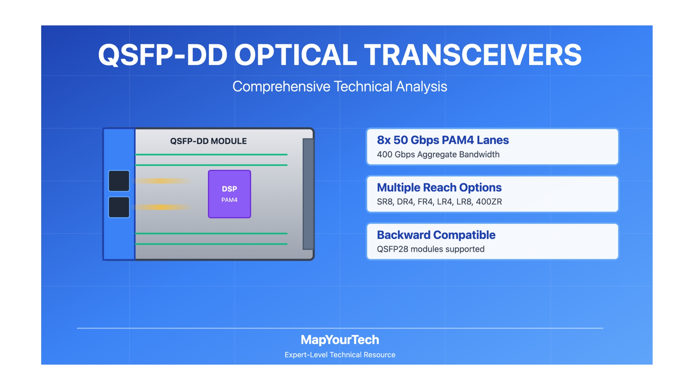
QSFP-DD technology builds upon the proven QSFP platform while doubling the number of electrical lanes from four to eight, enabling aggregate data rates of 400 Gbps and beyond. This evolutionary approach maintains backward compatibility with existing QSFP and QSFP28 modules while providing a clear migration path toward 800 Gbps and future higher-speed implementations. The form factor achieves this enhanced capability within the same physical footprint as previous generations, maximizing port density in space-constrained networking equipment.

The technical sophistication of QSFP-DD transceivers encompasses multiple domains: advanced electrical signaling utilizing Pulse Amplitude Modulation (PAM4) encoding, sophisticated thermal management systems to dissipate power densities exceeding 12-15 watts, high-speed serializer/deserializer (SerDes) circuits operating at 50-56 Gbps per lane, and comprehensive digital diagnostic capabilities conforming to the Common Management Interface Specification (CMIS). These integrated subsystems must operate cohesively within stringent power, thermal, and electromagnetic compatibility constraints.

Current market dynamics indicate robust adoption trajectories for QSFP-DD technology. Industry analysis projects the QSFP-DD pluggable optical transceiver market will reach approximately 8.5 billion USD by 2025, expanding at a compound annual growth rate of 22 percent through 2033. This growth is propelled by hyperscale data center expansion, the proliferation of 400 Gigabit Ethernet deployments, and increasing requirements for higher port densities in network switching infrastructure. The Asia-Pacific region is emerging as a dominant force in deployment, driven by extensive investments in 5G infrastructure and data center construction.

This comprehensive technical analysis examines QSFP-DD technology across multiple dimensions: historical evolution and standardization efforts, fundamental architectural principles, electrical and optical interface specifications, thermal management strategies, implementation methodologies, performance optimization techniques, practical deployment scenarios, and emerging trends including 800 Gbps coherent implementations. The discussion targets network engineering professionals, system architects, and technical decision-makers requiring detailed understanding of QSFP-DD capabilities, trade-offs, and best practices for successful deployment.

Scope and Objectives

This technical resource provides comprehensive coverage of QSFP-DD transceiver technology suitable for basic to expert-level practitioners in optical networking and telecommunications. The analysis emphasizes conceptual understanding of underlying principles, system-level architectural considerations, and practical implementation strategies rather than vendor-specific implementations or proprietary solutions.

Key learning objectives include understanding the electrical and optical interface specifications defined by the QSFP-DD Multi-Source Agreement, evaluating thermal management approaches for high-power transceivers, analyzing PAM4 signaling characteristics and forward error correction requirements, comparing various optical reach and application implementations, and developing deployment strategies optimized for specific network architectures and performance requirements.

Historical Context and Evolution

The Genesis of Pluggable Optical Transceivers

The evolution toward QSFP-DD technology represents the culmination of decades of innovation in pluggable optical transceiver design. The journey began with fixed-form-factor optical interfaces requiring complete equipment replacement for technology upgrades. The introduction of the Gigabit Interface Converter (GBIC) in the late 1990s marked the first significant shift toward hot-pluggable, field-replaceable optical modules, enabling network operators to upgrade optical interfaces without replacing entire chassis or line cards.

The Small Form-Factor Pluggable (SFP) transceiver, introduced in the early 2000s, reduced module size by approximately 50 percent compared to GBIC while maintaining electrical compatibility through the SFP Multi-Source Agreement (MSA). This standardization enabled multi-vendor interoperability and established the MSA framework as the preferred approach for defining new transceiver form factors. The SFP+ variant extended data rates to 10 Gbps per port, becoming the dominant interface for 10 Gigabit Ethernet applications.

The Quad Small Form-Factor Pluggable (QSFP) transceiver emerged to address the bandwidth scaling requirements of 40 Gigabit Ethernet, aggregating four 10 Gbps channels into a single module maintaining similar dimensions to the SFP+ form factor. This parallel architecture proved highly effective, with the QSFP+ variant supporting 40 Gbps aggregate throughput. The subsequent QSFP28 standard increased per-lane data rates to 25 Gbps, enabling 100 Gigabit Ethernet within the same mechanical envelope through a combination of electrical signaling improvements and manufacturing process refinements.

The QSFP-DD Development Timeline

The QSFP-DD MSA was formally established in 2016 to define a successor to QSFP28 capable of supporting 400 Gbps and higher data rates while maintaining maximum compatibility with existing infrastructure. The fundamental innovation involved doubling the electrical interface from four to eight high-speed lanes while preserving the module's horizontal dimensions and front panel footprint. This approach enabled backward compatibility: legacy QSFP28 modules can insert into QSFP-DD ports and connect to the lower four electrical lanes.

1998-2001
Introduction of GBIC and SFP transceiver standards, establishing pluggable optical interface paradigm and MSA-based standardization approach.
2006-2009
SFP+ standardization enabling 10 Gbps per port. QSFP development initiated for 40 Gigabit Ethernet applications using four-lane parallel architecture.
2013-2014
QSFP28 specification finalized, increasing per-lane data rates to 25 Gbps for 100 Gigabit Ethernet support. IEEE 802.3bm standard ratified.
2016
QSFP-DD MSA formally established with founding member companies. Initial specification work commenced focusing on eight-lane electrical interface supporting 400 Gbps aggregate throughput.
2017-2018
QSFP-DD hardware specification Version 1.0 and 2.0 released. IEEE 802.3bs 400 Gigabit Ethernet standard ratified, defining multiple QSFP-DD optical implementations.
2019-2020
Volume production of 400GBASE-SR8, DR4, FR4, and LR8 QSFP-DD modules commenced. CMIS 4.0 management interface specification adopted across industry.
2021-2022
Introduction of 400ZR coherent QSFP-DD implementations for data center interconnect. OpenZR+ MSA established for interoperable coherent transceivers.
2023-2024
Development of 800 Gbps QSFP-DD implementations utilizing 100 Gbps per lane PAM4 signaling. IEEE 802.3df 400GBASE-ZR standard completed.
2025-Present
Widespread deployment of 400G QSFP-DD across hyperscale data centers. Development of 800ZR+ coherent implementations and transition toward 1.6 Tbps optical interfaces.

The QSFP-DD hardware specification has undergone continuous refinement, with the current Version 4.0 incorporating lessons learned from field deployments and accommodating emerging requirements for higher power classes and enhanced thermal management. Parallel efforts in standards bodies, particularly the IEEE 802.3 Ethernet Working Group and the Optical Internetworking Forum (OIF), have defined complementary specifications for various optical implementations and coherent transmission technologies.

Competing and Complementary Form Factors

The QSFP-DD form factor exists within an ecosystem of competing and complementary transceiver standards, each optimized for specific deployment scenarios and performance requirements. The Octal Small Form-Factor Pluggable (OSFP) transceiver, developed concurrently with QSFP-DD, provides similar eight-lane electrical interface capabilities but with increased module volume enabling enhanced thermal dissipation for coherent optics implementations requiring higher power budgets.

The CFP, CFP2, CFP4, and CFP8 form factors target applications requiring maximum optical reach and performance without stringent size constraints, typically deployed in carrier-class equipment rather than high-density data center switches. The QSFP112 standard, introduced more recently, maintains four electrical lanes while increasing per-lane signaling rates to 112 Gbps, targeting 400 Gbps aggregate throughput with reduced electrical complexity compared to eight-lane architectures.

Market dynamics increasingly favor QSFP-DD for data center and enterprise networking applications due to its combination of high port density, backward compatibility advantages, and mature ecosystem support. Industry analyses indicate QSFP form factors including QSFP-DD will experience the highest compound annual growth rates through 2033, driven by widespread deployment in 400 Gigabit Ethernet and emerging 800 Gigabit Ethernet switching platforms.

Standardization Bodies and Specifications

QSFP-DD technology development involves collaboration across multiple standardization organizations. The QSFP-DD MSA defines mechanical specifications, electrical interfaces, thermal requirements, and management protocols. The IEEE 802.3 Working Group specifies Ethernet physical layer implementations including 400GBASE-SR8, DR4, FR4, LR8, and related variants. The OIF develops implementation agreements for coherent optics including 400ZR and provides guidance on interoperability testing.

The Common Management Interface Specification (CMIS), maintained by an industry consortium, defines the management interface for QSFP-DD and other high-speed transceivers. This two-wire serial interface provides access to module identification data, diagnostic monitoring capabilities, and configuration parameters. The latest CMIS revisions incorporate support for advanced features including firmware management, detailed performance monitoring, and adaptive equalization control.

Technical Architecture and System Design

Mechanical Form Factor Specifications

The QSFP-DD module mechanical design represents a carefully optimized balance between electrical performance, thermal management, manufacturability, and backward compatibility requirements. The module maintains the same horizontal dimensions as QSFP28 transceivers, measuring approximately 18.35 millimeters in width and 72.4 millimeters in depth, enabling deployment in existing equipment front panels designed for QSFP+ and QSFP28 modules.

The key mechanical innovation involves increased module height, expanding from approximately 8.5 millimeters for QSFP28 to 18.35 millimeters for QSFP-DD. This vertical expansion accommodates the double-density electrical connector incorporating eight high-speed differential pairs plus associated ground, power, and low-speed signaling contacts. The extended height also provides increased surface area for heat dissipation, critical for managing power dissipation levels reaching 12-15 watts in high-performance implementations.

The electrical connector system utilizes a 76-position edge connector featuring two rows of contacts, each row carrying four high-speed electrical lanes plus supporting infrastructure. The connector design incorporates ground-signal-signal-ground (GSSG) pin configuration optimizing signal integrity for 25-28 Gbaud PAM4 signaling rates per differential pair. Contact pitch and geometry are specified to achieve specified electrical performance through 30 Gbaud operation with defined insertion loss, return loss, and crosstalk characteristics.

QSFP-DD Module Physical Architecture
OPTICAL INTERFACE MODULE PCB OPTICAL SUBASSEMBLY (ROSA/TOSA) DSP / SerDes PAM4 Codec 8 x 50 Gbps CDR/Retimer Clock Recovery Equalization CONTROLLER MCU CMIS Management Interface MEMORY Configuration / Diagnostics 76-PIN CONNECTOR ≈ 72.4 mm (Module Depth) ≈ 18.35 mm (Module Height)

Electrical Interface Architecture

The QSFP-DD electrical interface implements an eight-lane differential signaling architecture, each lane capable of supporting data rates up to 28 Gbaud with PAM4 modulation, yielding 56 Gbps effective throughput per lane. The aggregate electrical bandwidth reaches 400 Gbps under standard operation, with the specification accommodating future expansion to 800 Gbps through increased per-lane signaling rates or alternative modulation schemes.

Each electrical lane consists of a differential pair operating with 85-ohm to 100-ohm differential impedance. The transmitter outputs conform to specifications derived from the IEEE 802.3cd 50GAUI-1 electrical interface, adapted for the QSFP-DD mechanical envelope. Typical differential output voltage swing ranges from 400 to 800 millivolts peak-to-peak, optimized for transmission through high-speed printed circuit board traces and connector systems while maintaining adequate noise margins.

The receiver electrical specification accommodates various equalization topologies including continuous-time linear equalization (CTLE), decision feedback equalization (DFE), and feed-forward equalization (FFE). These adaptive equalization techniques compensate for channel impairments including frequency-dependent attenuation, reflections, and inter-symbol interference accumulated across the electrical signal path. The receiver must achieve specified bit error rate performance, typically 1 × 10⁻¹² or better after forward error correction, across the full range of compliant channel implementations.

PAM4 Signaling Fundamentals

Pulse Amplitude Modulation with 4 levels (PAM4) encodes two bits of information per symbol using four distinct voltage levels rather than the two levels employed by traditional non-return-to-zero (NRZ) signaling. This approach doubles the effective bit rate compared to NRZ at the same baud rate, enabling 50 Gbps operation at approximately 26.5625 Gbaud symbol rate.

The four PAM4 voltage levels are typically designated as +3, +1, -1, and -3, representing bit patterns 11, 10, 00, and 01 respectively. The reduced voltage spacing between adjacent levels compared to NRZ signaling decreases signal-to-noise ratio by approximately 9.5 decibels theoretically. Practical implementations must employ sophisticated signal processing including precise level alignment, extensive equalization, and robust forward error correction to achieve acceptable bit error rates.

QSFP-DD Technical Article - Part 2 | MapYourTech

Optical Interface Implementations

QSFP-DD transceivers support diverse optical interface implementations optimized for specific reach requirements, fiber types, and deployment scenarios. These implementations represent carefully engineered trade-offs between cost, power consumption, optical reach, and complexity. The IEEE 802.3bs and 802.3cd standards define multiple 400 Gigabit Ethernet physical layer specifications accommodating multimode fiber data center applications, single-mode fiber campus and metropolitan networks, and long-haul coherent transmission systems.

Short-Reach Multimode Fiber Implementations

400GBASE-SR8 Specification

The 400GBASE-SR8 optical interface utilizes eight parallel optical lanes operating at 50 Gbps each over multimode fiber, achieving aggregate 400 Gbps throughput. Each optical lane employs an 850 nanometer Vertical-Cavity Surface-Emitting Laser (VCSEL) transmitter and corresponding PIN photodiode receiver. The parallel architecture distributes the high aggregate bandwidth across multiple lower-speed optical channels, simplifying per-lane optical component requirements while maintaining cost-effectiveness for short-reach applications.

Premium Article — Free 21% Preview

Read the Full Analysis with Premium

The remaining 79% of this article — the design numbers, trade-offs and field guidance — is part of MapYourTech Premium, along with the full premium library, courses and professional tools.
Instant access · Cancel anytime · 48-hour trial available
Sanjay Yadav

Optical Communications & Network Automation Expert | Author of 3 Books for Optical Engineers | Founder, MapYourTech

Optical networking engineer with nearly two decades of experience across DWDM, OTN, coherent optics, submarine systems, and cloud infrastructure. Founder of MapYourTech.

Follow on LinkedIn
Share:

You May Also Like

15 min read 14 0 Like Connector Types and Their Loss Budgets: SC, LC, MPO Skip to main content MapYourTech...
  • Free
  • July 11, 2026
16 min read 11 0 Like Cooled vs Uncooled Lasers: The Pluggable Power Trade-off Skip to main content MapYourTech |...
  • Free
  • July 11, 2026
16 min read 15 0 Like Automation Blast Radius: Scoping What a Bad Intent Can Touch Skip to main content...
  • Free
  • July 11, 2026

Course Title

Course description and key highlights

Course Content

Course Details