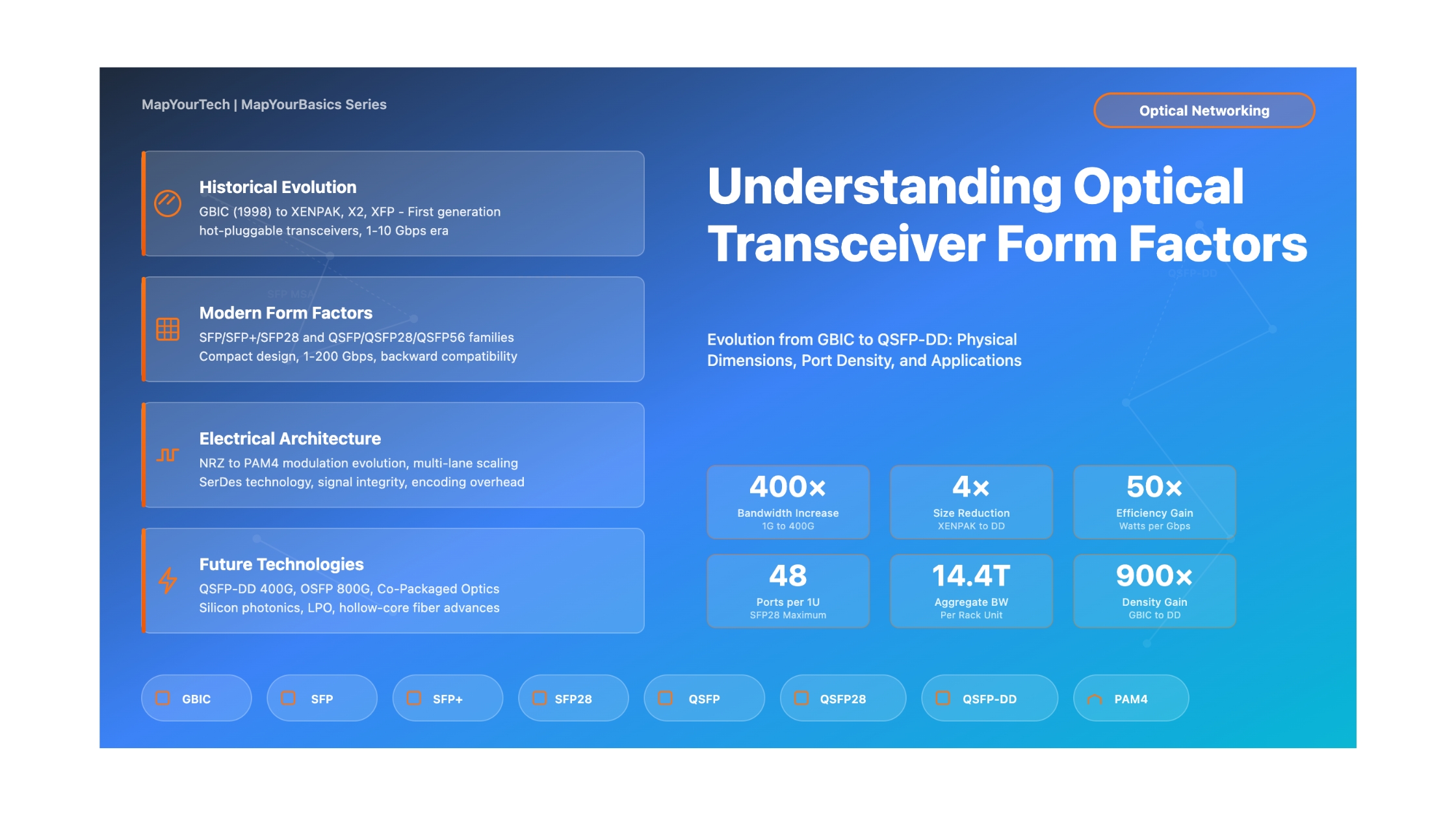

Understanding Optical Transceiver Form Factors: Evolution from GBIC to QSFP-DD
A Comprehensive Guide to Physical Dimensions, Port Density, and Use Cases Across Three Decades of Optical Networking Innovation
Introduction
Optical transceivers are the fundamental building blocks of modern fiber-optic networks, converting electrical signals to optical signals for transmission and vice versa for reception. Over the past three decades, the evolution of optical transceiver form factors has been driven by three key demands: higher port density, increased bandwidth, and reduced power consumption. This evolution represents one of the most significant engineering achievements in telecommunications, enabling the exponential growth of data center interconnects, metropolitan networks, and long-haul transmission systems.
Form factor refers to the physical size, shape, electrical interface, and mechanical mounting characteristics of optical transceivers. The journey from the original Gigabit Interface Converter (GBIC) in the late 1990s to today's Quad Small Form-factor Pluggable Double Density (QSFP-DD) modules supporting 400 Gigabits per second represents a revolution in packaging density. While the first-generation GBIC occupied approximately 80 cubic centimeters and delivered 1 Gigabit per second, modern QSFP-DD modules fit in less than 20 cubic centimeters while delivering 400 times the bandwidth.
This article provides a comprehensive technical examination of optical transceiver form factor evolution, covering physical dimensions, electrical interfaces, thermal management strategies, and deployment use cases. Network engineers, data center architects, and optical system designers will gain practical knowledge for selecting appropriate form factors based on port density requirements, power budgets, and bandwidth needs. We explore not only the current state of the technology but also the engineering trade-offs that shaped each generation of form factors.
The scope of this guide encompasses legacy form factors including GBIC, XENPAK, and X2; current mainstream technologies such as SFP, SFP+, SFP28, QSFP, QSFP28, and QSFP56; and emerging standards including QSFP-DD and OSFP. For each form factor, we examine mechanical specifications, electrical characteristics, thermal dissipation capabilities, and typical deployment scenarios. Understanding these fundamentals enables informed design decisions in network architecture, particularly as bandwidth demands continue to escalate and space constraints become more critical in modern data centers.
Figure 1: Evolution timeline showing the progression from legacy GBIC to modern QSFP-DD, with bandwidth increasing 400× while form factor size decreased 4×
1. Historical Background and Evolution
1.1 The Era Before Hot-Pluggable Transceivers
Before the introduction of hot-pluggable optical transceivers in the late 1990s, optical interfaces were typically soldered directly onto network equipment circuit boards or implemented as fixed-configuration modules. These early implementations presented significant limitations including lack of field upgradeability, limited optical reach options, and high costs for equipment replacement when optical interface requirements changed. The inability to swap optical interfaces without powering down equipment resulted in network downtime and operational complexity.
The telecommunications industry recognized the need for standardized, hot-pluggable optical transceivers that could be inserted and removed from active equipment without disrupting network operations. This requirement became particularly critical as Gigabit Ethernet emerged in the late 1990s, with multiple optical reach variants requiring different optical specifications. Network operators needed the flexibility to select appropriate optical modules based on specific link requirements while maintaining a common electrical interface on their switching and routing platforms.
1.2 GBIC: The First Standardized Hot-Pluggable Form Factor
The Gigabit Interface Converter (GBIC) emerged in 1998 as the first widely adopted hot-pluggable optical transceiver standard. Developed through a multi-source agreement (MSA) among leading network equipment vendors, GBIC defined a common mechanical, electrical, and functional specification that enabled interoperability across different vendor platforms. The GBIC form factor measured approximately 35mm × 65mm × 12mm, occupying roughly 80 cubic centimeters of volume.
GBIC modules featured a 20-pin edge connector for electrical interface with the host system and supported various optical configurations including short-reach multimode at 850nm, long-reach single-mode at 1310nm, and extended-reach single-mode at 1550nm. The modules provided SC duplex fiber connectors for optical connections, with transmit and receive fibers on separate connectors. GBIC power consumption typically ranged from 600 milliwatts to 1 watt, supplied by a single 3.3V or 5V rail.
While GBIC successfully solved the hot-pluggability challenge and enabled optical interface flexibility, its relatively large form factor limited port density on switch faceplates. A typical line card could accommodate approximately 12-16 GBIC ports in a standard rack unit, which became a significant constraint as network port densities increased. This limitation drove the development of smaller form factor solutions.
Important: GBIC Key Features
Physical Dimensions: 35mm (W) × 65mm (L) × 12mm (H) ≈ 27 cubic centimeters
Electrical Interface: 20-pin edge connector, 3.3V or 5V power supply
Optical Connectors: SC duplex (separate TX and RX)
Data Rate: 1.25 Gbps (Gigabit Ethernet, 1×Fiber Channel)
Typical Power: 600-1000 milliwatts
Port Density Limitation: ~12-16 ports per 1U line card
1.3 10 Gigabit Era: XENPAK, X2, and XFP
The introduction of 10 Gigabit Ethernet (10GbE) in 2002 through IEEE 802.3ae created new challenges for transceiver packaging. The 10× increase in data rate from Gigabit Ethernet required more sophisticated optical components, higher-performance electronic circuitry, and significantly improved thermal management. The first 10GbE transceiver form factor, XENPAK, was designed to accommodate these requirements but resulted in a physically large module.
XENPAK modules measured approximately 127mm × 82mm × 13mm, occupying nearly 135 cubic centimeters - substantially larger than GBIC. This size accommodated four-lane electrical interface (XAUI - 10 Gigabit Attachment Unit Interface), with each lane operating at 3.125 Gbps, and provided sufficient surface area for heat dissipation. XENPAK modules typically dissipated 4-6 watts, requiring active cooling in high-density applications. The 70-pin electrical connector provided power, data, and management interfaces.
The X2 form factor emerged in 2002 as a more compact alternative to XENPAK, reducing size to approximately 76mm × 40mm × 14mm (roughly 40 cubic centimeters). X2 maintained the same 70-pin XAUI electrical interface as XENPAK but achieved size reduction through tighter component integration and improved thermal design. The side-rail mounting system allowed heat dissipation optimization for different deployment environments including PCI cards, mid-board mounting, and front-panel applications.
XFP (10 Gigabit Small Form Factor Pluggable) represented a further miniaturization breakthrough, achieving dimensions of approximately 18mm × 76mm × 9mm (about 12 cubic centimeters). XFP integrated the XAUI-to-serial conversion circuitry within the module itself, presenting a single-lane 10.3125 Gbps serial electrical interface to the host system. This integration enabled significant size reduction but increased module complexity and power consumption to 2-4 watts. XFP became widely deployed in applications where port density was critical, such as high-capacity router line cards.
| Form Factor | Introduction Year | Dimensions (mm) | Volume (cm³) | Electrical Interface | Power (W) | Ports per 1U |
|---|---|---|---|---|---|---|
| XENPAK | 2001 | 127 × 82 × 13 | ~135 | XAUI (4×3.125G) | 4-6 | 4-6 |
| X2 | 2002 | 76 × 40 × 14 | ~43 | XAUI (4×3.125G) | 3-5 | 8-12 |
| XFP | 2003 | 18 × 76 × 9 | ~12 | Serial (10.3125G) | 2-4 | 24-32 |
1.4 The Small Form-Factor Revolution: SFP and SFP+
While GBIC addressed the hot-pluggability requirement for Gigabit Ethernet, the industry quickly recognized the need for higher port density. The Small Form-factor Pluggable (SFP) transceiver, introduced in 2001, represented a breakthrough in miniaturization. SFP modules reduced the physical footprint to approximately 13.5mm × 56mm × 8.5mm, roughly one-third the size of GBIC while maintaining the same 1.25 Gbps data rate. This size reduction enabled a doubling of port density on switch faceplates.
SFP utilized a 20-position edge connector similar to GBIC but with tighter pin spacing, enabling the compact form factor. The modules featured LC duplex optical connectors rather than SC connectors, with both transmit and receive fibers integrated into a single duplex connector housing. This connector choice further contributed to space savings. SFP power consumption ranged from 300 to 1000 milliwatts depending on optical reach, supplied by a 3.3V power rail.
The SFP form factor achieved immediate market acceptance and became the de facto standard for Gigabit Ethernet applications. By 2010, SFP had largely displaced GBIC in new equipment deployments. The SFP Multi-Source Agreement (MSA) established detailed mechanical, electrical, and thermal specifications, ensuring multi-vendor interoperability. The MSA also defined a digital diagnostic monitoring interface (DDMI) based on the SFF-8472 specification, enabling real-time monitoring of transceiver parameters including temperature, supply voltage, transmit optical power, and receive optical power.
SFP+ emerged in 2006 as the 10 Gigabit evolution of SFP, maintaining identical physical dimensions and mechanical interface while increasing the data rate to 10.3125 Gbps. This remarkable achievement - a 10× bandwidth increase in the same form factor - resulted from advances in integrated circuit technology, improved signal integrity design, and optimized optical component packaging. SFP+ presented a simplified electrical interface compared to earlier 10G form factors, using a single-lane SFI (Serdes Framer Interface) electrical specification rather than four-lane XAUI.
The SFP+ form factor rapidly gained adoption in 10 Gigabit Ethernet deployments, particularly in data center applications where port density was paramount. A single-rack-unit switch could accommodate 48 SFP+ ports, enabling 480 Gbps of aggregate bandwidth in a compact form factor. SFP+ modules supported diverse optical variants including 10GBASE-SR for multimode fiber at 850nm, 10GBASE-LR for single-mode at 1310nm, and 10GBASE-ER for extended reach at 1550nm. Direct attach copper (DAC) cables using the SFP+ form factor also emerged as cost-effective solutions for short-reach connections within racks.
Figure 2: SFP and SFP+ architectural comparison showing how identical mechanical form factor achieved 10× bandwidth increase through internal optimization
2. Modern High-Density Form Factors: QSFP Family Evolution
2.1 QSFP: Quad Small Form-factor Pluggable for 40 Gigabit
The Quad Small Form-factor Pluggable (QSFP) transceiver emerged in 2009 to address the bandwidth requirements of 40 Gigabit Ethernet. Rather than developing an entirely new form factor, the QSFP specification leveraged the proven SFP mechanical design philosophy while implementing a four-lane parallel electrical architecture. The QSFP form factor measures approximately 18mm × 72mm × 8.5mm, only marginally larger than SFP while delivering 40 Gbps aggregate bandwidth.
QSFP achieves 40 Gbps throughput by implementing four independent 10 Gbps electrical lanes, with each lane operating at 10.3125 Gbps to accommodate 64B/66B encoding overhead. The 38-position edge connector provides differential pairs for all four transmit lanes, all four receive lanes, plus power and management signals. This parallel architecture enables the use of proven 10G per lane optical and electrical components, reducing development risk and time-to-market compared to developing new 40G serial technology.
Multiple optical variants were developed for QSFP including 40GBASE-SR4 for multimode fiber using parallel 850nm VCSELs, 40GBASE-LR4 for single-mode fiber using wavelength division multiplexing of four wavelengths (1295nm, 1300nm, 1305nm, 1310nm), and 40GBASE-ER4 for extended reach. The SR4 variant utilizes MPO-12 connectors with 12 fibers (8 active, 4 spare) while LR4/ER4 variants use duplex LC connectors. Direct attach copper (DAC) cables and active optical cables (AOC) in QSFP format also gained significant market adoption for intra-rack and inter-rack connectivity.
QSFP power consumption ranges from 1.5 watts for short-reach SR4 modules to 3.5 watts for extended-reach variants, supplied by a 3.3V power rail. The increased power dissipation compared to SFP+ required enhanced thermal design, with most QSFP modules incorporating heat spreaders or fins for passive cooling. The QSFP MSA specification defined mechanical pull-tab and heat-sink clip designs to ensure adequate cooling in high-density applications.
QSFP Key Characteristics
Physical Dimensions: 18mm (W) × 72mm (L) × 8.5mm (H) ≈ 11 cubic centimeters
Data Rate: 4 × 10.3125 Gbps = 41.25 Gbps aggregate (40GbE with encoding)
Electrical Interface: 38-position edge connector, four differential TX/RX pairs
Optical Variants: SR4 (MPO-12, 850nm, 100-150m MMF), LR4 (LC, CWDM, 10km SMF), ER4 (LC, CWDM, 40km SMF)
Power Consumption: 1.5-3.5W depending on optical reach
Port Density: 36-48 ports per 1U switch (1.44-1.92 Tbps per rack unit)
2.2 SFP28 and QSFP28: The 25G and 100G Generation
The introduction of 25 Gigabit Ethernet in 2014 marked a strategic shift in data center networking economics. Rather than quadrupling bandwidth from 10G to 40G, the industry adopted a 2.5× step to 25 Gigabit per lane, enabling 100 Gigabit aggregate bandwidth with four lanes. This approach provided better cost scaling and power efficiency compared to 40G while delivering higher bandwidth. SFP28 and QSFP28 form factors emerged to support this new speed grade.
SFP28 maintains mechanical and electrical interface compatibility with SFP and SFP+, using the same 13.5mm × 56mm × 8.5mm dimensions and 20-position edge connector. The module increases the single-lane data rate from 10.3125 Gbps to 25.78125 Gbps (25GbE with 64B/66B encoding). This 2.5× bandwidth increase required advances in SerDes (Serializer/Deserializer) technology, improved signal integrity through better PCB design and connector performance, and enhanced optical components capable of the higher modulation bandwidth.
QSFP28 implements four lanes of 25 Gbps each, delivering 100 Gbps aggregate bandwidth in the same physical form factor as QSFP. The mechanical dimensions (18mm × 72mm × 8.5mm) and 38-position electrical connector remain identical to QSFP, with backward compatibility for 40G QSFP modules in QSFP28 ports (though not vice versa due to electrical signaling differences). This compatibility simplified network migrations and protected infrastructure investments.
QSFP28 optical variants include 100GBASE-SR4 for multimode fiber at 850nm using MPO-12 connectors (70-100m reach), 100GBASE-LR4 for single-mode at 1310nm using CWDM (10km reach), and 100GBASE-ER4 for extended reach at 1310nm CWDM (40km reach). The PSM4 (Parallel Single Mode 4-lane) variant uses parallel single-mode fibers on MPO-12 connectors for 500m to 2km applications. CWDM4 and LR4 specifications multiplex four wavelengths onto a single duplex LC connector, eliminating the need for MPO connectors in long-reach applications.
Power consumption for QSFP28 ranges from 2.5W for SR4 variants to 5.0W for long-reach modules with temperature control and wavelength stabilization. The higher power dissipation compared to QSFP required additional thermal management attention. Modern QSFP28 modules incorporate sophisticated thermal monitoring and typically implement thermal rollback algorithms that reduce transmit power if internal temperature thresholds are exceeded, protecting the module while maintaining link operation.
Figure 3: Physical size comparison of transceiver form factors showing the dramatic miniaturization from GBIC/XENPAK to modern QSFP-DD while bandwidth increased 400×
2.3 QSFP56 and the Path to 200 Gigabit
QSFP56 emerged in 2017 to support 200 Gigabit Ethernet by increasing the per-lane data rate from 25 Gbps to 50 Gbps. With four lanes operating at 50 Gbps each, QSFP56 delivers 200 Gbps aggregate bandwidth in the same mechanical form factor as QSFP28. This represents yet another doubling of capacity within an established package, demonstrating the continued effectiveness of the multi-lane parallel architecture.
The 50 Gbps per lane signaling required significant advances in SerDes technology and signal integrity engineering. PAM4 (4-level Pulse Amplitude Modulation) electrical signaling replaced the traditional NRZ (Non-Return-to-Zero) modulation used at lower speeds. PAM4 encodes two bits per symbol rather than one bit per symbol in NRZ, effectively doubling the data rate for a given baud rate. This approach reduced the frequency content of the electrical signal, making 50 Gbps per lane feasible within the electrical and thermal constraints of the QSFP form factor.
QSFP56 optical variants include 200GBASE-SR4 for multimode fiber, 200GBASE-DR4 for single-mode fiber at 1310nm, and 200GBASE-FR4 for extended reach. The PSM8 (Parallel Single Mode 8-lane) variant implements eight 25 Gbps lanes on parallel single-mode fibers for specific applications. Power consumption ranges from 3.5W for short-reach modules to 6.0W for long-reach variants with cooling and wavelength stabilization.
QSFP56 deployments have primarily focused on data center spine-leaf architectures where 200G provides an effective upgrade path from 100G without requiring changes to physical cabling infrastructure. The form factor compatibility with QSFP28 simplified adoption, as existing QSFP28 ports can typically support QSFP56 modules with appropriate host system ASIC support for PAM4 signaling.
2.4 QSFP-DD: Double Density for 400 Gigabit
The QSFP Double Density (QSFP-DD) form factor, standardized in 2019, addressed the challenge of supporting 400 Gigabit Ethernet while maintaining backward compatibility with existing QSFP28 infrastructure. QSFP-DD doubles the number of electrical lanes from four to eight while making minimal changes to the physical dimensions. The module measures 18.35mm wide × 78.5mm deep × 9.5mm tall, only marginally larger than QSFP28 (18mm × 72mm × 8.5mm).
QSFP-DD implements eight lanes of 50 Gbps PAM4 signaling, delivering 400 Gbps aggregate bandwidth. The mechanical design incorporates an innovative two-row electrical connector with 76 positions (compared to 38 in QSFP28), doubling the electrical interface capacity while preserving the module width. The connector pins are offset in two staggered rows, enabling the increased pin count without widening the form factor.
A critical feature of QSFP-DD is backward compatibility - QSFP28 and QSFP56 modules can plug into QSFP-DD ports, with the host system automatically detecting the module type and configuring the appropriate number of lanes. This compatibility protects infrastructure investments and simplifies network migrations. QSFP-DD ports can operate as a single 400G interface, two independent 200G interfaces, four independent 100G interfaces, or eight independent 50G interfaces, providing exceptional deployment flexibility.
QSFP-DD optical specifications include 400GBASE-SR8 for multimode fiber (using eight 50G lanes at 850nm), 400GBASE-DR4 for single-mode at 1310nm (using four 100G PAM4 lanes), and 400GBASE-FR4 for extended reach (also four 100G lanes). The ZR/ZR+ variants support coherent transmission for metro and regional networks, implementing digital signal processing for advanced modulation formats including 16QAM and polarization multiplexing.
Power consumption for QSFP-DD modules ranges from 6W for short-reach SR8 variants to 14W for long-reach coherent modules. This substantial power increase compared to earlier generations necessitated enhanced cooling solutions. The QSFP-DD MSA specifies improved heat sink interfaces and thermal monitoring capabilities, with most modules implementing dynamic power management that adjusts transmit power based on link budget requirements and thermal conditions.
Key Takeaways: QSFP Family Evolution
- Consistent Form Factor: QSFP, QSFP28, and QSFP56 maintain identical 72mm × 18mm × 8.5mm dimensions while increasing bandwidth from 40G to 200G through per-lane speed increases and modulation advances
- QSFP-DD Backward Compatibility: Minimal size increase (18mm to 18.35mm width, 8.5mm to 9.5mm height) enables plugging older QSFP modules into QSFP-DD ports, protecting infrastructure investments
- Parallel Architecture Scalability: Four-lane architecture scaled from 4×10G (40G) to 4×25G (100G) to 4×50G (200G), with QSFP-DD extending to eight lanes for 400G
- PAM4 Modulation Enabler: Transition from NRZ to PAM4 signaling at 50 Gbps per lane enabled bandwidth doubling while managing electrical signal integrity and power consumption
- Deployment Flexibility: QSFP-DD supports breakout modes including 2×200G, 4×100G, and 8×50G, maximizing utilization across different network topologies
3. Technical Architecture and Electrical Interface Evolution
3.1 Electrical Interface Standards
The electrical interface between optical transceivers and host systems has evolved significantly across generations, driven by increasing data rates and the need for backward compatibility. Early form factors like GBIC used parallel 8B/10B encoded data lanes at relatively low speeds (1.25 Gbps), while modern transceivers implement high-speed serial interfaces with 64B/66B encoding and advanced modulation schemes.
SFP and SFP+ modules implement a differential CML (Current Mode Logic) electrical interface operating at 1.25 Gbps and 10.3125 Gbps respectively. The interface consists of transmit and receive differential pairs with specified impedance (typically 100 ohms differential) and voltage levels. The SFF-8431 specification defines the electrical characteristics including rise/fall times, jitter requirements, and eye diagram masks that ensure signal integrity across different vendor implementations.
QSFP family modules utilize the CAUI (40 Gigabit Attachment Unit Interface) specification for four-lane signaling, with each lane carrying 10.3125 Gbps in QSFP, 25.78125 Gbps in QSFP28, or 50 Gbps in QSFP56. The QSFP-DD specification extends this to eight lanes. The electrical interface includes AC coupling capacitors within the module to isolate DC levels between the host system and transceiver, minimizing ground loop issues and enabling hot-pluggability without electrical transients.
3.2 Management Interface and Digital Diagnostics
Modern optical transceivers implement sophisticated management interfaces that enable real-time monitoring and control. The foundation of this capability is the I2C (Inter-Integrated Circuit) two-wire serial interface, operating at 100 kHz or 400 kHz clock rates. Through this interface, host systems can access EEPROM memory within the transceiver containing identification, capability, and real-time diagnostic information.
The Digital Diagnostic Monitoring Interface (DDMI), specified in SFF-8472 for SFP and SFF-8636 for QSFP, provides real-time access to critical operating parameters. Monitored parameters include module temperature, supply voltage, laser bias current, transmit optical power, and receive optical power. Each parameter includes programmable alarm and warning thresholds, enabling proactive fault detection before link failures occur.
Advanced modules implement additional capabilities including tunable laser wavelength control, transmit power adjustment, receive equalization settings, and Forward Error Correction (FEC) statistics. These controls enable network operators to optimize link performance based on specific fiber characteristics and link budgets. The management interface supports both passive monitoring and active link optimization.
3.3 Power Management and Thermal Considerations
Power consumption and thermal management represent critical design constraints for optical transceivers, particularly as data rates and port densities increase. Early GBIC modules consuming 600-1000 milliwatts at 1 Gbps have evolved to QSFP-DD modules dissipating up to 14 watts at 400 Gbps - a 14× power increase for a 400× bandwidth increase, demonstrating improving power efficiency on a per-bit basis.
The power supply architecture has remained relatively consistent across generations, with most modules operating from a 3.3V power rail supplied by the host system. Internal DC-DC converters generate the various voltage levels required for laser drivers, transimpedance amplifiers, and digital circuitry. Modern modules implement sophisticated power management including soft-start circuitry to limit inrush current, power-good signaling to the host, and low-power modes for standby operation.
Thermal management challenges scale with power consumption. Short-reach modules operating at 2-3 watts typically rely on passive cooling through the module housing and heat spreader designs. Long-reach modules dissipating 6-14 watts require active cooling, with heat sinks designed to interface with switch chassis airflow. The QSFP-DD MSA defines enhanced heat sink clip mechanisms to ensure adequate thermal coupling between module and switch heat sink.
Temperature monitoring within modern transceivers enables intelligent thermal management strategies. Modules implement temperature-dependent transmit power adjustment to maintain consistent optical power output as laser characteristics vary with temperature. Critical temperature thresholds trigger alarm conditions, and extreme temperatures can activate thermal shutdown protection to prevent component damage. Typical operating temperature ranges span 0°C to 70°C for commercial-grade modules and -40°C to 85°C for extended-temperature industrial variants.
Figure 4: Electrical interface evolution showing progression from simple parallel NRZ signaling to advanced PAM4 modulation with enhanced management capabilities
4. Performance Optimization and Port Density Economics
4.1 Port Density Comparison Across Generations
Port density - the number of network interfaces per rack unit of equipment - directly impacts data center capital efficiency and operational costs. The evolution from GBIC to modern QSFP-DD represents a transformative improvement in space utilization. A typical 1U switch with GBIC ports accommodated 12-16 ports delivering 12-16 Gbps aggregate bandwidth, while modern 1U switches with 36 QSFP-DD ports deliver 14.4 Tbps - a 900× improvement in bandwidth density.
The SFP form factor breakthrough enabled 24-48 ports per 1U at Gigabit speeds, doubling or quadrupling the port count compared to GBIC. SFP+ maintained this density at 10 Gigabit speeds, with high-density switches supporting 48 ports per 1U delivering 480 Gbps aggregate. The compact size of SFP/SFP+ modules enabled dense front-panel mounting without requiring exotic cooling solutions, making these configurations economically viable.
QSFP family modules trade individual port count for aggregate bandwidth - a 1U switch typically supports 32-36 QSFP-DD ports (compared to 48 SFP28 ports), but each QSFP-DD port delivers 400 Gbps versus 25 Gbps for SFP28. This results in 12.8-14.4 Tbps aggregate bandwidth per 1U for QSFP-DD compared to 1.2 Tbps for SFP28. The larger QSFP form factor accommodates higher power modules and provides space for enhanced cooling interfaces.
Port Density and Aggregate Bandwidth Evolution
4.2 Power Density and Cooling Requirements
Power density - watts dissipated per rack unit - has emerged as a critical constraint in data center design. While individual transceiver power consumption has increased with data rates, power efficiency on a per-bit basis has improved significantly. A 1U switch with 48 GBIC ports (1 watt each) dissipated approximately 48 watts for 48 Gbps, or 1 watt per Gbps. Modern switches with 36 QSFP-DD ports (8 watts each) dissipate approximately 288 watts for 14.4 Tbps, or 0.02 watts per Gbps - a 50× improvement in power efficiency.
This power density increase requires sophisticated thermal management. Legacy equipment with low-power transceivers relied primarily on chassis ambient airflow. Modern high-density switches implement directed airflow architectures with faceplate-to-rear or side-to-side airflow patterns, ensuring adequate cooling for transceiver modules. Fan speed control based on temperature sensors in both the switch ASIC and optical modules optimizes acoustic noise while maintaining thermal margins.
The industry has developed standardized cooling approaches for different power classes. Modules consuming less than 3.5 watts typically use passive cooling through module housing and switch faceplate heat sinking. Modules dissipating 3.5-6 watts require enhanced passive cooling with heat spreaders and thermal interface materials. Modules exceeding 6 watts necessitate active cooling coordination between module thermal design and switch chassis airflow architecture.
4.3 Cost per Gigabit Analysis
Understanding the economic drivers of form factor evolution requires examining the total cost of ownership across the network stack. Initial transceiver costs represent only one component - network operators must also consider switch port costs, fiber plant costs, rack space costs, and operational expenses including power and cooling. Form factor miniaturization has enabled favorable scaling across all these dimensions.
Legacy GBIC modules delivering 1 Gbps typically cost $300-500 per port in the early 2000s, resulting in $300-500 per Gbps. Modern SFP28 modules delivering 25 Gbps cost approximately $100-150 per port, or $4-6 per Gbps - a 50-75× cost reduction. QSFP-DD modules at $800-1200 per port deliver 400 Gbps, yielding $2-3 per Gbps. This dramatic cost improvement has enabled the exponential bandwidth growth of internet infrastructure.
Switch silicon costs also benefit from port miniaturization. A 1U switch with 48 SFP28 ports shares a common switching ASIC across all ports, with the ASIC cost amortized over 1.2 Tbps of capacity. Larger form factors like QSFP-DD enable even better ASIC cost scaling - 36 ports sharing switch silicon cost across 14.4 Tbps. The trend toward fewer, higher-bandwidth ports with compact form factors improves both transceiver and switch economics.
| Form Factor | Ports per 1U | Aggregate BW | Power per Port | Total Power | W/Gbps | Approx. $/Gbps |
|---|---|---|---|---|---|---|
| GBIC | 12-16 | 12-16 Gbps | 0.6-1.0 W | ~12 W | 1.0 | $300-500 |
| SFP | 24-48 | 24-48 Gbps | 0.3-1.0 W | ~24 W | 0.5-1.0 | $100-200 |
| SFP+ | 24-48 | 240-480 Gbps | 1.0-1.5 W | ~60 W | 0.125-0.25 | $20-40 |
| SFP28 | 48 | 1.2 Tbps | 1.0-1.5 W | ~72 W | 0.06 | $4-6 |
| QSFP28 | 32-36 | 3.2-3.6 Tbps | 3.5-5.0 W | ~160 W | 0.05 | $3-5 |
| QSFP-DD | 32-36 | 12.8-14.4 Tbps | 6-12 W | ~288 W | 0.02 | $2-3 |
5. Emerging Technologies and Future Directions
5.1 OSFP: Optimizing for 800G and Beyond
The Octal Small Form Factor Pluggable (OSFP) represents an alternative approach to the 400G and 800G challenge. Rather than minimizing form factor changes as QSFP-DD did, OSFP prioritizes thermal management and electrical performance by adopting a moderately larger package. OSFP measures 22.6mm wide × 107mm deep × 9mm tall, providing approximately double the surface area of QSFP-DD for heat dissipation while remaining compact enough for high-density deployments.
OSFP implements an eight-lane electrical architecture like QSFP-DD but with enhanced thermal interfaces. The larger form factor accommodates improved heat sink attachment mechanisms and provides space for higher-power optical engines. OSFP modules support 400G using eight lanes at 50 Gbps PAM4, and the specification roadmap includes 800G using eight lanes at 100 Gbps PAM4 and eventually 1.6T using eight lanes at 200 Gbps.
The OSFP MSA emphasizes forward compatibility and thermal headroom. The specification includes provisions for modules dissipating up to 15 watts without requiring exotic cooling solutions, positioning OSFP for coherent optics and advanced modulation formats that demand higher DSP power. Industry adoption of OSFP has focused on hyperscale data center applications where the thermal advantages justify the modest size increase compared to QSFP-DD.
5.2 Co-Packaged Optics (CPO) and Silicon Photonics Integration
Co-packaged optics represents a revolutionary departure from pluggable transceiver modules, instead integrating optical engines directly onto the switch ASIC package substrate. This approach eliminates the electrical reach limitations and power consumption of high-speed SerDes interfaces by positioning optical components within millimeters of the switch silicon. Early CPO implementations target 51.2 Tbps switch ASICs with integrated 64×800G or 128×400G optical interfaces.
CPO leverages silicon photonics technology to fabricate optical components including modulators, photodetectors, and wavelength multiplexers using standard semiconductor manufacturing processes. The optical engines mount directly on the switch package substrate, with electrical connections through microbumps or wire bonds rather than high-speed SerDes interfaces. This integration reduces power consumption by 30-50% compared to pluggable optics while enabling higher port densities.
The transition to CPO introduces new challenges including field serviceability (optical engines are no longer hot-swappable), fiber management (fiber connections directly to switch package rather than faceplate modules), and qualification complexity (optical and electrical testing must occur at switch package level). Despite these challenges, the power and density advantages position CPO as a likely architecture for next-generation hyperscale data centers operating at 800G and 1.6T per port.
5.3 Linear Pluggable Optics (LPO) and Lower-Power Solutions
Linear Pluggable Optics (LPO) represents an alternative approach to power reduction by eliminating DSP-based retiming and equalization from optical modules. Traditional pluggable transceivers incorporate retiming CDR (Clock and Data Recovery) circuits and feed-forward equalization to condition electrical signals from the host system before optical transmission. These DSP functions consume 30-40% of module power in modern 400G implementations.
LPO modules replace DSP circuitry with simple linear driver amplifiers, relying on the host system SerDes to provide signal conditioning and timing recovery. This approach reduces module power consumption from 8-10 watts to 4-5 watts for 400G QSFP-DD applications, enabling passive cooling in many deployments. The trade-off involves increased host system power consumption and reduced electrical reach - LPO typically limits host-to-module electrical connections to 100-200mm PCB trace lengths.
LPO finds application in data center spine-leaf architectures where electrical reach constraints are manageable and power savings directly reduce cooling costs. The approach represents an optimization point between pluggable optics (maximum reach but higher power) and CPO (maximum integration but reduced serviceability). Industry adoption of LPO accelerated in 2023-2024 as hyperscale operators pursued aggressive power reduction targets.
5.4 Hollow-Core Fiber and Future Optical Innovations
While this article focuses primarily on transceiver form factors, emerging fiber technologies will influence future module designs. Hollow-core fiber - where light propagates through air-filled cores rather than glass - promises dramatically reduced latency (approaching 99% the speed of light in vacuum compared to 67% for standard fiber) and nearly zero chromatic dispersion. These characteristics could enable simplified optical modules without the extensive DSP currently required for dispersion compensation.
Advanced modulation formats including probabilistic constellation shaping and multidimensional modulation will push transceiver DSP complexity higher, potentially increasing module power consumption. Form factor evolution may need to accommodate these processing requirements while maintaining or improving power efficiency. The industry continues to explore options including in-module AI accelerators for adaptive equalization and modulation optimization.
Key Takeaways: Future Form Factor Trends
- OSFP Thermal Headroom: 2× surface area compared to QSFP-DD enables 800G-1.6T roadmap with manageable thermal dissipation, supporting power-hungry coherent optics and advanced DSP
- CPO Paradigm Shift: Moving optical engines onto switch ASIC package reduces SerDes power by 30-50% and enables higher port densities, but sacrifices field serviceability of traditional pluggable modules
- LPO Power Optimization: Eliminating module-side DSP reduces power consumption from 8-10W to 4-5W for 400G applications, enabling passive cooling with trade-off of reduced electrical reach to ~100-200mm
- Bandwidth Scaling: Industry roadmap targets 800G deployments in 2026-2027 and 1.6T by 2028-2029, likely requiring either larger form factors (OSFP) or integration approaches (CPO) to manage thermal challenges
- Silicon Photonics Maturation: Integration of optical components using semiconductor processes enables CPO while reducing manufacturing costs, with potential to eventually replace discrete optics in pluggable modules
6. Practical Application Guidance and Selection Criteria
6.1 Selecting Appropriate Form Factors for Different Applications
Choosing the optimal transceiver form factor requires evaluating multiple factors including required bandwidth, port density constraints, power budget limitations, thermal environment, and optical reach requirements. Different network segments have distinct optimization points that favor specific form factors.
Access layer switches typically prioritize port density and cost per port over raw bandwidth, making SFP and SFP28 ideal choices. These deployments often involve many lower-bandwidth connections to end devices, and the compact SFP form factor maximizes the number of ports in limited rack space. SFP28 at 25 Gbps provides ample bandwidth for uplinks while maintaining high port counts for server or WiFi access point connections.
Distribution and aggregation layers balance port density against aggregate bandwidth requirements. QSFP28 modules delivering 100 Gbps match well with typical distribution layer designs, providing adequate bandwidth for aggregating multiple access layer uplinks while supporting reasonable port densities. The option to break out QSFP28 ports into 4×25G connections using AOCs or fiber fanout cables provides deployment flexibility.
Spine and core network segments prioritize maximum bandwidth over port count, favoring QSFP-DD at 400 Gbps or emerging 800G options. These deployments typically involve fully meshed connectivity between spine and leaf switches, where fewer high-bandwidth links provide better switch silicon utilization than many lower-bandwidth connections. The larger physical size of QSFP-DD modules presents minimal challenges in spine switches that typically populate only a fraction of available faceplate positions.
Form Factor Selection Guidelines
Choose SFP/SFP28 when:
- Maximum port density is critical (48 ports per 1U)
- Bandwidth per port ≤ 25 Gbps is sufficient
- Power budget favors lower-power modules (1-1.5W each)
- Application: Access layer, ToR (Top of Rack), server connectivity
Choose QSFP28/QSFP56 when:
- Moderate port density (32-36 ports per 1U) with 100-200 Gbps per port
- Breakout capability required (4×25G or 4×50G)
- Power budget allows 3.5-6W per module
- Application: Distribution layer, aggregation, leaf switches
Choose QSFP-DD when:
- Maximum bandwidth per port (400 Gbps) is priority
- Port count 24-36 per 1U is acceptable
- Power budget supports 6-12W per module with active cooling
- Application: Spine switches, DCI (Data Center Interconnect), backbone
6.2 Interoperability and Multi-Vendor Considerations
Multi-Source Agreements (MSAs) define mechanical, electrical, and management interfaces to ensure interoperability across vendors. However, practical deployment requires attention to several compatibility considerations. Host system support for specific data rates and modulation formats varies - not all QSFP28 ports support backward compatibility with QSFP modules, and QSFP-DD port capabilities differ across switch platforms.
Optical specifications may vary subtly between vendor implementations while remaining MSA-compliant. Fiber type compatibility, connector keying, transmit power ranges, and receive sensitivity specifications should be verified between paired transceivers. Direct attach copper cables are particularly vendor-specific, as cable lengths, gauge, and equalization characteristics must match the host system's electrical specifications.
Digital diagnostic monitoring interfaces provide a valuable tool for verifying transceiver operation and compatibility. After installing modules, network operators should verify temperature, voltage, and optical power measurements fall within normal ranges. Unexpected alarm conditions often indicate compatibility issues such as inadequate cooling, incorrect power supply voltage, or optical power mismatches.
6.3 Migration Strategies and Backward Compatibility
Network upgrades typically occur incrementally rather than wholesale replacements. Understanding form factor compatibility enables cost-effective migration paths. QSFP-DD ports accept QSFP28 and QSFP modules, enabling gradual bandwidth increases without replacing switch infrastructure. Similarly, SFP28 ports typically accept SFP+ and SFP modules, though not all platforms support auto-negotiation to lower speeds.
Breakout cables provide another migration tool - a single QSFP28 port can break out to four separate SFP28 connections using appropriate fiber fanout or active optical cables. This approach maximizes utilization of existing switch ports during transitions from 10G to 25G server connectivity. However, breakout configurations consume multiple SerDes lanes on the switch ASIC, potentially reducing the total achievable bandwidth.
Planning for future upgrades should consider not only current bandwidth requirements but also power infrastructure and cooling capacity. Upgrading from QSFP28 to QSFP-DD may require cooling system enhancements to accommodate the increased power dissipation. Infrastructure investments in power distribution and cooling should target the expected future state rather than just current needs.
7. Conclusion
The evolution of optical transceiver form factors from GBIC to QSFP-DD represents a remarkable engineering achievement spanning three decades. Physical volume has decreased by a factor of four while bandwidth has increased by a factor of 400, resulting in a 1600× improvement in bandwidth density. This transformation enabled the explosive growth of cloud computing, streaming media, and modern internet applications that would be impossible with legacy technologies.
Several key principles emerge from this historical analysis. First, standardization through Multi-Source Agreements proved essential for industry-wide adoption and cost reduction through competition. Second, incremental evolution within established form factors (SFP → SFP+ → SFP28) provided superior economics compared to revolutionary redesigns, as existing infrastructure and expertise could be leveraged. Third, parallel lane architectures enabled practical scaling to higher bandwidths using proven per-lane technologies rather than requiring fundamental breakthroughs.
Looking forward, the industry faces fundamental challenges as bandwidth requirements continue escalating. Power density already approaches physical limits in air-cooled environments, and electrical SerDes interfaces face diminishing returns as data rates exceed 100 Gbps per lane. Co-packaged optics and silicon photonics integration represent promising paths forward, but introduce new trade-offs in serviceability and qualification complexity.
For network architects and engineers, understanding form factor evolution provides essential context for technology selection and infrastructure planning. The progression from 1 Gbps to 400 Gbps occurred over 20 years (1998-2018), but the next jump to 800 Gbps and beyond may occur in just 5-7 years. Planning for this accelerating pace requires not only selecting appropriate current technologies but also ensuring infrastructure flexibility to accommodate future generations.
The optical transceiver form factor landscape continues to evolve, driven by the relentless demand for higher bandwidth, improved power efficiency, and reduced costs. The technologies and trends described in this article provide a foundation for understanding both the current state of the art and the likely trajectory of future innovations. Success in optical networking requires not only technical knowledge but also appreciation for the economic, thermal, and practical constraints that shape technology evolution.
References and Further Reading
- SFF Committee, "SFF-8472 Specification for Diagnostic Monitoring Interface for Optical Transceivers"
- QSFP-DD MSA, "SFF-8665 QSFP+ 28 Gb/s 4X Pluggable Transceiver Solution"
- IEEE 802.3ba, "IEEE Standard for Ethernet - Amendment 4: Media Access Control Parameters, Physical Layers, and Management Parameters for 40 Gb/s and 100 Gb/s Operation"
- IEEE 802.3bs, "IEEE Standard for Ethernet - Amendment 10: Media Access Control Parameters, Physical Layers, and Management Parameters for 200 Gb/s and 400 Gb/s Operation"
- OIF (Optical Internetworking Forum), "Implementation Agreement for Integrated Dual Polarization Intradyne Coherent Receivers"
- QSFP-DD MSA, "QSFP Double Density 8X Pluggable Transceiver"
- OSFP MSA, "Octal Small Formfactor Pluggable Module"
- COBO (Consortium for On-Board Optics), "Co-Packaged Optics Specification"
- Sanjay Yadav, "Optical Network Communications: An Engineer's Perspective" - Bridge the Gap Between Theory and Practice in Optical Networking
Developed by MapYourTech Team
For educational purposes in Optical Networking Communications Technologies
Note: This guide is based on industry standards, best practices, and real-world implementation experiences. Specific implementations may vary based on equipment vendors, network topology, and regulatory requirements. Always consult with qualified network engineers and follow vendor documentation for actual deployments.
Feedback Welcome: If you have any suggestions, corrections, or improvements to propose, please feel free to write to us at [email protected]

Optical Communications & Network Automation Expert | Author of 3 Books for Optical Engineers | Founder, MapYourTech
Optical networking engineer with nearly two decades of experience across DWDM, OTN, coherent optics, submarine systems, and cloud infrastructure. Founder of MapYourTech. Read full bio →
Follow on LinkedIn