
Co-Packaged Optics: Architecture, Status, and the Path to 1.6T Switches
An advanced technical examination of how electrical bandwidth limits are reshaping switch design, the silicon photonics architectures at the core of CPO, external laser source strategies, COBO and OIF specifications, and the industry roadmap toward 1.6T and beyond.
1. Introduction
The economics and physics of data center networking are converging on a single conclusion: the traditional model of pluggable optical transceivers, separated from the switch Application-Specific Integrated Circuit (ASIC) by centimeters of printed circuit board trace, cannot continue to scale. As per-port speeds advance from 800 Gb/s toward 1.6 Tb/s and beyond, the electrical signaling losses between the ASIC and the optical module consume an increasing fraction of total system power and constrain the practical density of switch systems.
Co-Packaged Optics (CPO) addresses this by relocating the optical conversion function — the point at which electrical signals become photons — from a pluggable module at the front panel to a position directly adjacent to, or integrated within, the switch ASIC package. The result is a dramatic reduction in the length of high-speed electrical traces that must carry 100 Gb/s, 200 Gb/s, or 400 Gb/s signals, and a corresponding reduction in the power required to overcome those losses.
CPO is not a single technology but a family of integration approaches, ranging from modules mounted on the same substrate as the ASIC to full photonic-electronic monolithic integration. As of 2026, the industry has reached an inflection point: CPO has progressed from conference demonstrations to commercial deployments at hyperscale operators, with two of the largest switch ASIC vendors shipping or sampling first-generation products. Major AI infrastructure operators are selecting CPO for specific scale-up and scale-out workloads, and a new set of multi-source agreements (MSAs) is reshaping the ecosystem.
This article provides a thorough technical treatment of CPO: the physical limits that drive it, the silicon photonics architecture at its core, the standards and MSA landscape governing it, the specific design challenges engineers face, and the deployment roadmap through the 1.6T generation and into the 400 Gb/s per lane era.
2. The Electrical Bandwidth Problem
2.1 PCB Insertion Loss at High SerDes Rates
A switch ASIC communicates with a pluggable optical module through PCB traces called SerDes channels — Serializer/Deserializer lanes. Each lane carries a high-speed serial data stream. In current 200 Gb/s PAM4 implementations, the Nyquist frequency is approximately 26–28 GHz. At these frequencies, PCB insertion loss is dominated by the skin effect and dielectric absorption, and scales roughly with the square root of frequency and linearly with trace length.
// Simplified PCB channel insertion loss model:
IL ≈ α_d × L × √f
Where:
IL = insertion loss [dB]
α_d = loss coefficient [dB / (m × GHz^0.5)]
L = trace length [meters]
f = frequency [GHz]
// Typical values on standard FR4 PCB:
α_d ≈ 0.4 to 0.8 dB/(inch × GHz^0.5)
// For a 200 Gb/s PAM4 lane at 26 GHz Nyquist, 6-inch trace:
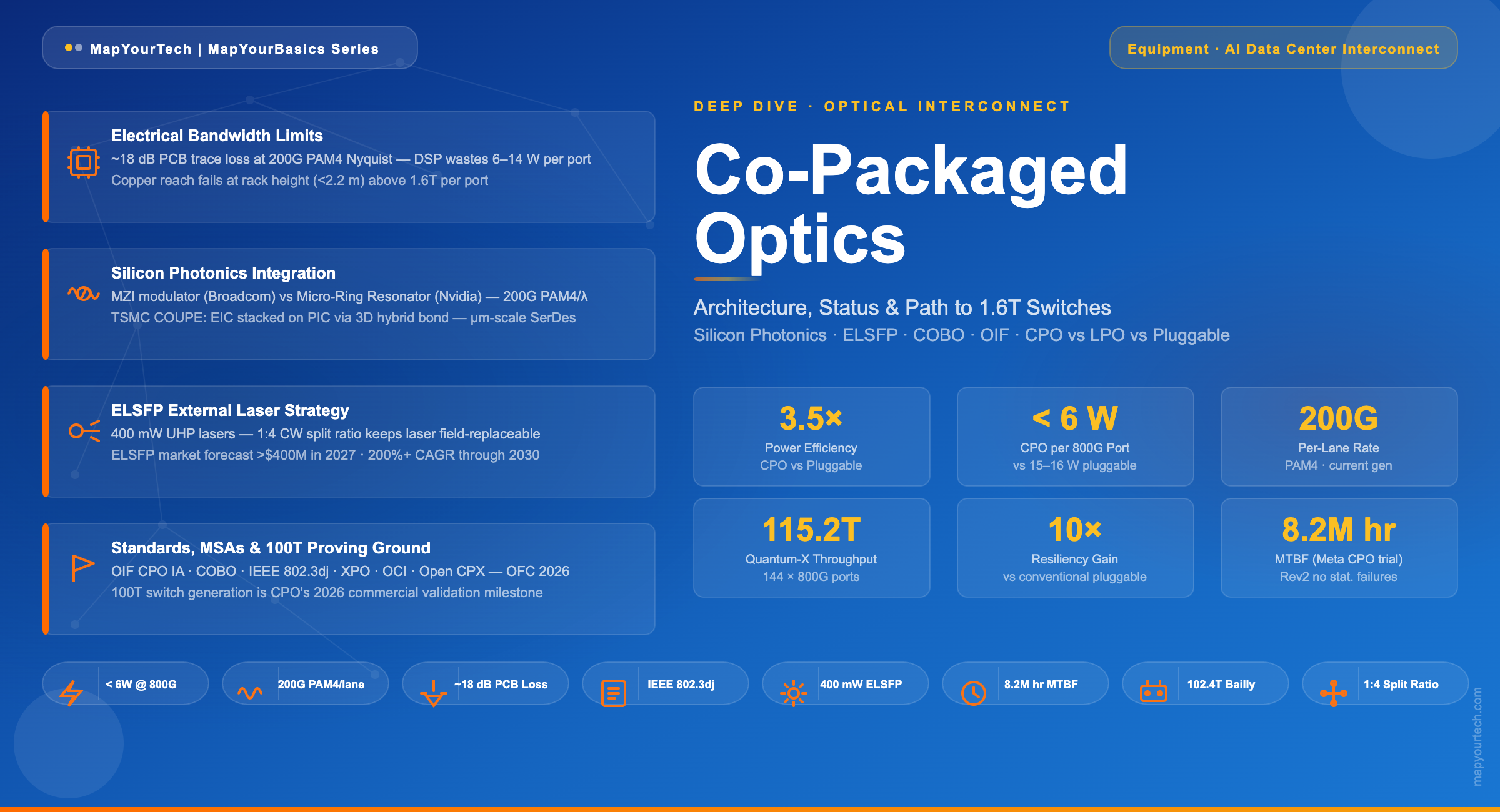
IL ≈ 0.6 × 6 × √26 ≈ 18.3 dB ← requires DSP equalization to recoverTo recover signal integrity across a loss budget of this magnitude, the system requires a Digital Signal Processor (DSP) inside the pluggable module. That DSP typically consumes 6–7 W for a single 800G module, and 12–14 W for a 1.6T module. At the scale of a large AI training cluster with tens of thousands of ports, this DSP overhead accumulates to hundreds of kilowatts of power that does no useful data switching — it only compensates for avoidable electrical losses.
One analysis of a large GPU cluster found that DSP equalization power for the back-end network alone could reach approximately 480 kW for an 18,000-accelerator system, or about 1.8 kW per server rack. When conventional pluggable modules are sourced from premium suppliers, they can account for nearly 10% of a cluster's total cost of ownership.
Key insight: DSPs in pluggable modules exist primarily to compensate for electrical channel losses between the ASIC and the front panel. Shortening that electrical path eliminates most of the loss — and most of the need for a DSP.
2.2 The Bandwidth×Reach Product of Copper
Copper electrical interconnects face a fundamental bandwidth-distance product limit. As per-port speeds advance, the maximum reach over which copper can operate — with or without active retiming — shrinks. At 400 Gb/s, retimed copper cables reach approximately 6 meters; passive copper drops to about 3 meters. At 800 Gb/s, retimed copper falls below standard rack height (2.2 m) for passive cables. At 1.6 Tb/s, even retimed copper reaches of approximately 1 meter are projected, making inter-rack connectivity impossible without optical media.
This physical reality defines CPO's opportunity: at 1.6T, optical links are required between racks. At 3.2T, optical links will be needed within racks. CPO provides the density and power profile to serve this growing optical demand without the DSP overhead of conventional pluggables.
Figure 1: Maximum reach of copper interconnect technologies versus per-port speed. At 1.6T, passive copper cannot span a standard rack height (2.2 m), making optical the only viable inter-rack option. Source: derived from industry data (Lumentum, OFC 2026).
- PCB insertion loss at 200 Gb/s PAM4 Nyquist frequencies can exceed 18 dB on a 6-inch trace, requiring DSP equalization that consumes 6–14 W per module.
- DSP power at cluster scale accumulates to hundreds of kilowatts of non-switching overhead.
- Copper reach shrinks with speed: at 1.6T, passive copper cannot span rack height, mandating optics.
- CPO eliminates most of the electrical path length, removing the loss that justifies DSP use.
3. What CPO Is — and Is Not
3.1 The Integration Spectrum
CPO describes a range of integration strategies, not a single packaging technology. The industry has converged on three broad categories based on how closely optics and electronics are combined:
On-Board Optics (OBO)
The optical module is removed from the front-panel cage and soldered or socketed onto the main board, directly adjacent to the switch ASIC. The Consortium for On-Board Optics (COBO), founded in 2015, developed form-factor and electrical interface specifications for this category. Electrical traces are shorter than front-panel pluggable, but the optical engine is still a separate component from the ASIC.
Near-Packaged Optics (NPO)
The optical engine sits on the same package substrate as the switch ASIC — separated by millimeters rather than centimeters. Electrical interconnect within the package uses bump bonds or fine-pitch wire bonds rather than PCB traces, reducing lane loss substantially. NPO is sometimes called "socketed CPO" when the engine uses a connector interface for replaceability.
True Co-Packaged Optics (CPO)
The photonic integrated circuit (PIC) and the electronic integrated circuit (EIC) share the same package — potentially the same silicon die area via wafer bonding or 2.5D/3D integration. Electrical interconnects between the ASIC and the modulator or detector are measured in micrometers to tens of micrometers. This is the approach used by both major switch ASIC vendors in their current implementations.
CPO and Linear Pluggable Optics (LPO) are both implementation variants of the same core idea: reduce the power consumed by ASIC-to-optics signal processing. LPO removes the DSP from a pluggable module and moves signal equalization to the ASIC's own transmit SerDes output, while the module operates in a fully linear receive mode. CPO takes a more radical step by eliminating the pluggable form factor entirely and co-locating the photonic conversion hardware on the ASIC package. The two technologies are complementary: LPO serves inter-rack distances where pluggability and multi-vendor interoperability are priorities, while CPO serves applications where maximum power and density efficiency justify a more integrated, less field-serviceable approach.
3.2 The Transponder Layer
In a conventional switch system, a pluggable transceiver performs electrical-to-optical conversion, houses a DSP, and manages the interface between the switch ASIC's SerDes and the optical fiber. In CPO, this transponder function migrates into the switch package itself. The optical fiber attaches directly to the package via a fiber attachment unit (FAU), and the laser source is provided externally via an External Laser Small Form-factor Pluggable (ELSFP) module at the front panel. This architectural shift is sometimes described as "eliminating the transponder layer" — though more accurately, it relocates and distributes those functions rather than removing them entirely.
4. Silicon Photonics Foundations
4.1 Why Silicon Photonics
Silicon photonics (SiPho) uses standard CMOS fabrication infrastructure to build optical waveguides, modulators, photodetectors, and multiplexers on a silicon-on-insulator (SOI) substrate. This compatibility with semiconductor manufacturing gives SiPho two decisive advantages for CPO: extreme geometric precision (sub-micron feature sizes allow dense photonic integration) and the ability to co-fabricate or closely integrate photonic circuits with electronic logic using the same foundry equipment.
The refractive index contrast between silicon (n ≈ 3.45 at 1.55 µm) and its oxide cladding (n ≈ 1.45) creates strong optical confinement in sub-micron waveguides, enabling tight bends with radii of a few micrometers and dense photonic routing. This compactness is what allows hundreds of optical channels to be routed on a chip area measured in square millimeters.
4.2 Modulator Architectures: MZI vs. Micro-Ring
The choice of optical modulator architecture is one of the most consequential design decisions in a CPO system, with significant implications for power, bandwidth, thermal sensitivity, and yield. As of 2026, the two dominant approaches used in commercial CPO switches are Mach-Zehnder Interferometer (MZI) modulators and micro-ring resonator (MRR) modulators.
| Parameter | Mach-Zehnder Modulator (MZI) | Micro-Ring Resonator (MRR) |
|---|---|---|
| Operating principle | Plasma dispersion effect changes refractive index in two arms; interference controls output power | Resonant coupling controlled by plasma dispersion; on-resonance couples light to ring, off-resonance passes through waveguide |
| Device footprint | Large — MZI arms typically 0.5–1 mm long; millimeter-scale | Small — ring diameter 5–20 µm; can be tightly arrayed |
| Bandwidth | High intrinsic electrical bandwidth; less sensitive to photon lifetime limits | Limited by photon lifetime in the resonator; typical 3-dB bandwidth of 10–30 GHz per ring |
| Drive voltage | High — typically 2–4 Vpp per arm for full modulation | Low — milliwatt-level tuning range; sub-volt drive typical |
| Insertion loss | Higher — 3–6 dB with splitters/combiners | Lower in through port when off-resonance; ~0.5–1 dB through loss |
| Temperature sensitivity | Low — broadband; resonance not relevant | High — ring shifts ~80 pm/°C; requires thermal control or tracking |
| Power consumption | Higher driver power due to voltage requirements | Lower modulation power, but thermal tuning adds overhead |
| Wavelength selectivity | Wideband — operates across a broad wavelength range without tuning | Narrowband — each ring selects a specific wavelength, enabling WDM per ring |
| Vendor choice (as of 2026) | Broadcom (Bailly platform) | Nvidia (Quantum-X, Spectrum-X platforms) |
Table 1: MZI vs. micro-ring modulator comparison for silicon photonics CPO applications.
Nvidia's micro-ring modulator silicon photonics engine achieves 200 Gb/s PAM4 modulation per wavelength with an ultra-compact footprint enabled by TSMC's COUPE (Chip on Wafer on Substrate with Photonics Enhanced) process, which stacks an electronic die (EIC) directly atop a photonics die using 3D hybrid bonding. This achieves extremely short interconnects between drive electronics and the modulator, which is essential for maintaining signal integrity at 200 Gb/s. The tradeoff is thermal sensitivity: Nvidia's optical engines require active thermal control and operate under liquid cooling.
Broadcom's Bailly platform uses MZI-based modulators, which are less thermally sensitive and more compatible with air-cooled or conventional liquid-cooled environments. The Bailly chip integrates 6.4 Tb/s silicon-photonics-based optical engines inside the ASIC package, with 16 pluggable laser modules providing continuous-wave light via fiber patch cords.
4.3 Photodetectors and Waveguide Routing
On the receiver side, SiPho uses germanium-on-silicon photodetectors, which achieve responsivities of approximately 1 A/W at 1310 nm and are compatible with standard CMOS processing. Waveguide routing on the photonic die uses single-mode silicon waveguides with tight bends enabled by the high index contrast. At the die boundary, waveguides transition to edge couplers or grating couplers that interface with the external fiber attachment unit. Edge couplers achieve lower coupling loss (typically 1–2 dB) and broader spectral bandwidth than grating couplers, making them the preferred interface for high-density, broadband CPO applications.
5. CPO Architecture in Detail
5.1 Optical Engine Structure
An optical engine (OE) in a CPO context is the sub-assembly that performs the electro-optical conversion for a defined number of optical channels. In both major commercial implementations as of 2026, each optical engine handles 1.6 Tb/s of bidirectional capacity using eight 200 Gb/s PAM4 transmit lanes and eight 200 Gb/s PAM4 receive lanes, for a total I/O capacity of 3.2 Tb/s full duplex per engine. Each transmit lane consumes light from an external laser source, modulates it using the on-chip modulator, and routes the optical signal to the fiber attachment unit. Each receive lane couples incoming light from fiber into the on-chip waveguide, routes it to a germanium photodetector, and outputs a photocurrent to the transimpedance amplifier (TIA) in the EIC.
5.2 Optical Subassembly (OSA) and Fiber Attachment
In Nvidia's Quantum-X implementation, three optical engines are clustered into a detachable optical subassembly (OSA) that provides 4.8 Tb/s of transmit and 4.8 Tb/s of receive bandwidth. Each OSA mates with the switch package substrate via a mechanical interface. This approach makes the optical engines — and their fiber interfaces — replaceable without disturbing the switch ASIC itself. It represents a practical compromise between the integration density of true CPO and the field serviceability concerns that initially slowed CPO adoption.
Each engine operates on eight 200 Gb/s PAM4 transmit lanes and eight 200 Gb/s PAM4 receive lanes, with two laser input fiber connections per engine. The Quantum-X switch uses 24 such engines in total, organized into eight OSAs, delivering 144 × 800 Gb/s ports and 115.2 Tb/s of aggregate switching capacity.
The fiber attachment unit (FAU) at the edge of the optical engine converts between on-chip waveguides and fiber, typically using a precisely aligned fiber array bonded to the chip edge. Insertion loss at this interface is a key yield and performance parameter, with edge-coupler-based FAUs achieving typically 1–2 dB coupling loss per channel.
6. External Laser Sources — ELSFP
6.1 Why Lasers Must Stay External
Lasers are the highest-reliability-risk component in any optical system. They degrade over time, can fail suddenly, and are sensitive to temperature. Integrating lasers permanently into the switch ASIC package would mean that a laser failure requires replacing the entire switch — an unacceptable operational model for a data center asset costing tens of thousands of dollars. The industry consensus, confirmed by OIF implementation agreements, is to keep the laser source external and pluggable while co-packaging everything else.
The External Laser Small Form-factor Pluggable (ELSFP) is the module that delivers continuous-wave (CW) laser light into the optical engines via fiber. The laser itself resides in the ELSFP; fiber patch cords connect the ELSFP front-panel port to the FAU of each optical engine on the package. When a laser degrades, the ELSFP is replaced without touching the switch ASIC or its co-packaged optics.
6.2 ELSFP Power Evolution
The optical power delivered by an ELSFP must be sufficient to feed all the modulators it serves after splitting and waveguide losses. In the 200 Gb/s PAM4 generation, each ELSFP typically drives four optical engines using a 1:4 optical splitter on the PIC. The first ELSFP modules contracted for Nvidia's scale-up switches produced 200–250 mW of optical output. As optical engine density increased, suppliers moved to 400 mW devices — a level now available from multiple InP-based laser manufacturers. This level is commonly described as Ultra High Power (UHP) in supplier materials. Lumentum has additionally demonstrated 800 mW devices targeting future implementations where higher split ratios would reduce the total number of ELSFP slots required per system. These higher-power devices are described as Super High Power (SHP).
Multiple sources at OFC 2026 confirmed that a 1:4 split ratio will remain standard for the next 2–3 years. As of 2026, Lumentum is shipping 400 mW UHP ELSFPs; Coherent is also shipping 400 mW units manufactured using 6-inch InP wafer capability. The ELSFP module market is forecast to exceed $400 million annually by 2027, with compound annual growth rates exceeding 200% from 2025 to 2030 by certain supplier estimates.
Note on meta-reliability: Meta Platforms reported at ECOC 2025 and confirmed with additional data at OFC 2026 that their deployed CPO switch system achieved a mean time between failure (MTBF) of 8.2 million hours, approximately 10 times that of the pluggable-based comparison system in the same trial. Failures were traced to a manufacturing defect in a specific ELSFP revision, which was corrected in the next hardware generation. The second-generation deployment accumulated over 50 million operating hours without statistically significant failures.
6.3 Multi-Wavelength ELSFP
Current ELSFPs deliver a single, fixed wavelength of CW light, which is then split and distributed to multiple engines. For future WDM-based CPO implementations — where each ring modulator selects a specific wavelength from a comb source — multi-wavelength ELSFPs become relevant. Lumentum demonstrated 16-wavelength UHP ELSFPs at OFC 2026, targeting future multi-wavelength (e.g., FR-type optical reach) CPO implementations. Genuine Optics also showed an 8-wavelength comb laser approach for CPO at the same event. These multi-wavelength sources would allow a single ELSFP to serve WDM channels on multiple rings simultaneously, increasing the bandwidth-per-ELSFP ratio and reducing front-panel slot consumption.
Figure 3: ELSFP optical output power progression and supported split ratio by generation. As output power grows, fewer ELSFP modules are needed per switch, reducing front-panel slot consumption and system cost. Data from OFC 2026 industry presentations.
7. Standards: COBO and OIF
7.1 COBO — Consortium for On-Board Optics
COBO was founded in 2015, led by Microsoft, to create common interface specifications for optical modules installed directly on the main board rather than at the front panel. The consortium grew to more than 60 participants including system equipment manufacturers, optical module companies, and electrical interconnect companies. COBO defined three form-factor classes for on-board modules, with different physical sizes supporting different thermal management approaches across a range of power consumption levels.
On the electrical interface side, COBO specified two interface types. The first is an eight-lane interface based on IEEE 400GAUI-8, designed for 400 Gb/s applications using eight 50 Gb/s PAM4 signals. The second is a 16-lane version for 800 Gb/s modules using sixteen 50 Gb/s PAM4 signals. COBO also anticipated that once IEEE defined 100 Gb/s lane signals, these interfaces would naturally scale to 800 Gb/s and 1.6 Tb/s. COBO provided important industry learning about on-board integration challenges — thermal management, fiber handling, serviceability models — even though it never achieved broad commercial adoption.
7.2 OIF CPO Framework
The Optical Internetworking Forum (OIF) has been the primary industry standards body for CPO specifications. The OIF CPO framework documents define functional partitioning between the host switch and the optical engine, the optical and electrical interfaces between them, and management and telemetry requirements. OIF implementation agreements for the ELSFP form factor define the mechanical, electrical, and optical specifications for the external laser source module, including power levels, fiber interface geometry, and management interface protocols.
The OIF also defines the Common Electrical I/O (CEI) specifications that govern the electrical interface between the switch ASIC SerDes output and the optical engine input. For CPO applications, the relevant CEI generation defines signaling parameters for the ultra-short, on-package electrical links — different from the long-reach CEI parameters used for conventional pluggable module interfaces. These on-package interfaces carry signals over micrometer- to millimeter-scale distances, allowing much higher signal integrity than any PCB-based channel.
7.3 IEEE 802.3 Standards Supporting CPO
Several IEEE 802.3 task forces define the Ethernet MAC, PCS, and PMD layers that CPO systems must implement:
- IEEE 802.3df defines 200G, 400G, and 800G Ethernet PMDs at 100 Gb/s per lane — the generation that includes 800G-DR8 and comparable interfaces used in current CPO switch implementations.
- IEEE 802.3dj defines 200G, 400G, 800G, and 1.6T Ethernet PMDs at 200 Gb/s per lane — the generation directly relevant to 1.6T port-speed CPO switches and the lane rate used by Nvidia's current COUPE-based optical engines.
- UCIe (Universal Chiplet Interconnect Express) is a die-to-die interface standard relevant to chiplet integration models where the optical engine is packaged as a chiplet alongside the switch ASIC.
| Standard / Body | Scope | CPO Relevance |
|---|---|---|
| OIF CPO Framework IA | Functional partitioning, host/OE interfaces, management | Primary CPO system specification |
| OIF ELSFP IA | External laser module form factor, power, fiber interface | Defines pluggable laser source for CPO |
| OIF CEI (on-package) | On-package electrical I/O for ASIC-to-OE link | Governs µm-scale SerDes interface inside package |
| COBO On-Board Optics Spec | On-board module form factors, 400GAUI-8 / 16-lane interfaces | Historical precursor; defined serviceability models |
| IEEE 802.3df | 200G/400G/800G Ethernet at 100 Gb/s per lane | PMDs for current 800G-port CPO switches |
| IEEE 802.3dj | 200G/400G/800G/1.6T Ethernet at 200 Gb/s per lane | PMDs for 1.6T-port CPO switches |
| UCIe | Die-to-die chiplet interconnect standard | Relevant for optical engine chiplet integration |
Table 2: Standards framework governing CPO system design and interoperability.
- COBO specified on-board optics form factors and electrical interfaces using IEEE 400GAUI-8 and 16-lane variants, providing early learning for the industry.
- OIF CPO Framework IAs define the functional boundary between the switch ASIC and optical engine, including on-package electrical interfaces and management protocols.
- OIF ELSFP IA standardizes the pluggable external laser source form factor and performance requirements.
- IEEE 802.3dj (200 Gb/s per lane) is the PMD standard directly applicable to 1.6T-port CPO switch designs.
8. Design Trade-offs and Challenges
8.1 Thermal Management
Placing photonic components inside or immediately adjacent to a switch ASIC creates a severe thermal environment. Switch ASICs at 51.2T and 102.4T switching capacity dissipate 300–500 W or more. Silicon photonic modulators — particularly micro-ring resonators — have resonance frequencies that shift with temperature at a rate of approximately 80 pm/°C. At the internal temperatures of a switch package, this thermal drift can shift rings off-resonance entirely if not actively compensated.
Both major CPO vendors have adopted liquid cooling as standard for their CPO switch platforms. The Nvidia Quantum-X photonic switch uses two liquid-cooled CPO chips. Broadcom's Bailly-based deployments also operate under liquid cooling. This is not merely a preference — the thermal dissipation densities involved (multiple hundred watts per package) are not manageable with air cooling at the speeds required for CPO operation. As liquid cooling infrastructure becomes standard in AI data centers, this constraint aligns with the broader infrastructure direction, though it does create a dependency that limits CPO deployment to environments with appropriate cooling.
For micro-ring implementations specifically, active thermal tuning circuits are embedded in the EIC to maintain ring resonance across temperature. Each ring requires a local heater and a wavelength-locking feedback loop, consuming additional power — typically a few milliwatts per ring — as an overhead against the modulation power savings.
8.2 Serviceability and the Failure Mode Problem
The largest operational objection to CPO has historically been serviceability. In a pluggable architecture, any individual module can be replaced in seconds without affecting adjacent ports or the switch ASIC. In CPO, the optical engines are co-located on the switch package, and in some implementations they are permanently bonded.
The industry has responded with two strategies. First, ELSFP modules keep the highest-failure-probability component (the laser) at the front panel, where it is accessible and replaceable. Second, some vendors have introduced detachable optical subassembly (OSA) designs — as Nvidia has done with the Quantum-X — where the three-engine OSA can be disconnected from the package and replaced as a field-replaceable unit, though this requires accessing the inside of the switch chassis rather than simply hot-swapping a front-panel module.
Meta's operational data from its CPO trial provides the most substantial public evidence on reliability. After addressing a manufacturing defect in early ELSFP units, the system achieved MTBF values far exceeding those of comparable pluggable-based systems. Oracle's public position is that high-quality fixed lasers are intrinsically more reliable than pluggable lasers and that pluggability itself introduces mechanical wear as a failure mechanism — suggesting that some operators may eventually prefer permanently integrated laser sources for their reliability advantages.
8.3 Manufacturing Yield and Cost
Co-packaging photonics with switch silicon introduces yield challenges that do not exist for standalone ASICs. A switch ASIC at advanced process nodes (4 nm, 3 nm) already has finite die yield. Adding a photonic die, whether through 3D bonding, flip-chip, or wafer-on-wafer stacking, means that a defect in either the electronic or photonic die results in a combined-package failure. This multiplicative yield risk increases the effective cost per good unit and constrains the economics of CPO relative to pluggable modules, particularly at lower production volumes.
As CPO volume scales — and as TSMC and other advanced packaging foundries refine COUPE and comparable processes — yields are expected to improve. Broadcom's Bailly and Nvidia's Quantum-X represent first commercial generations where these yield risks are real but manageable. The 100T switch generation, expected to be the proving ground for CPO at volume, will reveal whether yields are sufficient for broad hyperscale deployment.
8.4 Fiber Density and Plant Management
CPO switches terminate fiber directly at the package rather than at a pluggable module with a standard form factor. This shifts fiber management from a standardized front-panel pluggable interface to a more complex package-level fiber attachment. MPO connectors and fiber array units (FAUs) are used, but the higher fiber counts per switch — compared to an equivalent number of individual pluggable modules — require careful planning of cable routing, connector accessibility, and cleaning procedures.
9. CPO vs. LPO vs. Conventional Pluggable
Engineers designing AI data center interconnects in 2026 choose among four primary technology categories: conventional pluggable (with DSP), Linear Pluggable Optics (LPO), Co-Packaged Optics (CPO), and active copper-based solutions for the shortest reaches. Each has a distinct power-reach-flexibility trade-off profile.
| Parameter | Conventional Pluggable (DSP) | Linear Pluggable (LPO) | Co-Packaged Optics (CPO) |
|---|---|---|---|
| Typical power @ 800G | 15–16 W per module | 8–9 W per module | <6 W per port |
| DSP in optical path | Yes — in pluggable module | No — DSP offloaded to ASIC SerDes Tx | No — eliminated or ASIC-integrated |
| Optical reach | Up to 2,000 m (DR4, FR4) | Up to 2,000 m (with host-side Tx EQ) | Typically same as DSP-free pluggable when fiber-connected |
| Field replaceability | Full — hot-swap front panel | Full — standard OSFP/QSFP-DD | Partial — ELSFP replaceable; OE requires chassis access |
| Multi-vendor interop | High — standardized form factors | Moderate — LPO MSA required; ASIC interop varies | Low — closely coupled to switch ASIC design |
| Cooling requirement | Air-cooled standard | Air-cooled standard | Liquid cooling required for current implementations |
| Deployment maturity | High — billions of units in field | Ramping — early deployments in 2025–2026 | Early — first commercial deployments 2025–2026 |
| Primary use case (2026) | Scale-out, general-purpose DCI | Short-reach scale-out where ASIC supports linear Tx | Scale-up AI clusters; dense hyperscale switching |
Table 3: Technology comparison at 800G per-port speed. CPO delivers the lowest power per port but at the cost of reduced field replaceability and tighter vendor coupling.
Practical guidance: For scale-out AI fabric deployments in 2026, 800G LPO or conventional pluggable remains the mainstream choice due to multi-vendor availability and operational familiarity. CPO is the targeted choice for scale-up AI cluster switching where maximum power efficiency and density justify the operational complexity, and where the switch and optical engine are sourced from a tightly integrated vendor ecosystem.
10. Deployment Status and Industry Progress
10.1 Broadcom Bailly Platform
Broadcom has pursued CPO development since its first public announcements in 2021. The company's Bailly platform — based on its Tomahawk 6 Ethernet switch ASIC — integrates 6.4 Tb/s silicon-photonics-based optical engines inside the ASIC package, with 16 pluggable laser modules (two per optical engine) delivering CW light via fiber. As of 2026, Broadcom is shipping the Bailly platform to early access customers and partners. The Micas Networks company has been named as a partner delivering a volume production CPO switch based on the Broadcom architecture.
Broadcom's approach uses MZI-based modulators, which are less thermally sensitive than micro-rings and compatible with a wider range of liquid-cooling implementations. The system supports 102.4 Tb/s of switching capacity in an optically enabled configuration. A 409.6 Tb/s configuration using four CPO packages is also planned.
Broadcom demonstrated good post-FEC error rate performance from its CPO-based modulators at OFC 2026, which is particularly important for AI traffic patterns where sustained error-free operation is a functional requirement.
10.2 Nvidia Quantum-X and Spectrum-X
Nvidia announced its Quantum-X InfiniBand photonic switch and Spectrum-X Ethernet photonic switch at GTC 2025. The Quantum-X, targeted at InfiniBand-based AI scale-up clusters, delivers 115.2 Tb/s total throughput across 144 ports of 800 Gb/s using 24 optical engines built on TSMC's COUPE process. Each engine uses micro-ring modulators operating at 200 Gb/s PAM4 per wavelength. Only 18 ELSFP laser modules are needed for the entire switch — each ELSFP feeds light to eight 1.6 Tb/s photonic engines — representing approximately four times fewer laser modules per unit bandwidth compared to competing architectures.
The Spectrum-X photonic switch targets Ethernet-based scale-out connectivity, delivering 400 Tb/s total throughput from 512 ports in one configuration. Hardware for Spectrum-X was expected from manufacturing partners in the second half of 2026. Nvidia has emphasized that the CPO technology provides a 3.5-times power efficiency improvement and a 10-times resiliency improvement compared to previous switch generations with conventional pluggables, the latter attributable primarily to the drastically reduced laser count and the use of 3D-packaged, co-optimized components.
10.3 The 100T Generation as the Proving Ground
Each major switch vendor is preparing both pluggable and CPO/NPO options for the 100T switch generation, allowing customers to choose based on their specific operational requirements. Industry analysts view the 100T generation as CPO's definitive validation test. If CPO succeeds at this scale, the 200T generation would be the first where CPO is expected to surpass pluggable optics in deployed port count. If CPO does not achieve broad adoption at 100T, the industry trajectory would extend the coexistence of multiple technologies and packaging approaches for another product generation.
11. New MSA Landscape at OFC 2026
OFC 2026 saw the launch of three new multi-source agreements, each directly or indirectly shaped by the CPO transition. Their simultaneous emergence reflects the industry's recognition that the pluggable paradigm, CPO, and near-packaged optics are all viable in different deployment segments, and that standards infrastructure is needed for each.
11.1 XPO MSA
XPO is designed to extend pluggable optics into liquid-cooled environments, allowing high-density pluggable modules to compete with CPO in data centers where liquid cooling is available. By targeting liquid cooling, XPO enables substantially higher power budgets per module than air-cooled OSFP or QSFP-DD, which in turn allows higher-performing pluggable optics at distances and densities that previously required CPO. The XPO launch received broad industry acknowledgment and is viewed as a direct competitive response to CPO's power density advantage in liquid-cooled AI data centers.
11.2 OCI — Optical Chiplet Interconnect
OCI (Optical Chiplet Interconnect) standardizes a scale-up CPO interface — an optical connection standard between chiplets where the lane rate is defined at lower speed (effectively sub-200 Gb/s per wavelength) but using WDM to deliver aggregate bandwidth matching or exceeding 200 Gb/s per lane architectures. OCI uses an 8-wavelength source and transmits bidirectionally over two fibers. The MSA is backed by Broadcom, Meta, Nvidia, and AMD. The value proposition is a power or cost advantage over straight 200 Gb/s PAM4 approaches for specific short-reach scale-up distances where WDM over lower-baud-rate wavelengths is more efficient. Marvell is notably absent from OCI, likely due to architectural differences related to micro-ring implementations.
11.3 Open CPX
Open CPX defines a connectorized interface for near-packaged optics and socketed CPO. It specifies a standardized connector and module format that can be used for both NPO and CPO applications. The core value of Open CPX is that it allows operators to choose their optical engine supplier independently of the switch ASIC supplier — addressing the lock-in concern that makes some customers hesitant about fully integrated, vertically sourced CPO solutions. Whether this represents a differentiated market opportunity or whether the tightly integrated economics of vertically coupled CPO will dominate remains to be seen from adoption data.
| MSA | Target Application | Key Backers | Primary Value |
|---|---|---|---|
| XPO | High-density liquid-cooled pluggable | Broad industry | Extends pluggable into liquid-cooled DC environments; competitive with CPO |
| OCI | Scale-up CPO, chiplet optical I/O | Broadcom, Meta, Nvidia, AMD | Standardizes WDM-based short-reach optical chiplet interconnect |
| Open CPX | Socketed CPO / NPO | Multiple | Connectorized CPO enabling multi-source OE procurement |
Table 4: New MSAs launched at OFC 2026 related to CPO and high-density pluggable optics.
12. Roadmap to 400G/Lane and Beyond
12.1 The 400G/Lane Era
As of 2026, the CPO generation in deployment uses 200 Gb/s per lane electrical interfaces between the switch ASIC and the optical engine. The next generation advances to 400 Gb/s per lane. Broadcom debuted its Taurus platform DSP at OFC 2026, which accepts 200 Gb/s per lane electrical inputs and delivers 400 Gb/s per lane optical output — effectively a 4-lane 1.6T transceiver DSP. The Taurus platform also enables a path to 3.2T optical modules for the generation following. The significance for CPO is that the on-package SerDes running at 400 Gb/s per lane would double the bandwidth per optical engine at the same fiber count, allowing CPO switch capacity to scale from ~100T to ~200T without proportionally increasing package size or fiber count.
Industry forecasts anticipate that more than 100 million units of 1.6T and 3.2T optical transceivers will ship over the next five years, with close to half using 400G per lane optics. The 400G per lane era also sets the foundation for 3.2T pluggable modules, which would use 8 lanes of 400G optical output — and for 204.8T switching capacity in a single RU system with CPO.
12.2 The Feynman Rack and Scale-Up CPO
Nvidia's roadmap includes the Feynman rack platform, targeted for 2028, which will incorporate CPO-based scale-up connectivity between accelerators within a rack rather than just at the switch level. In this architecture, CPO links appear not only between spine switches but within the compute domain itself — connecting accelerators, HBM memory chiplets, and switches through a coherent photonic fabric. This represents the most aggressive integration phase of the CPO roadmap and, if successful, would make CPO the standard interconnect fabric across the entire AI rack from switch to accelerator.
12.3 The Three-Phase Lumentum Model
Lumentum's publicly presented model for CPO evolution describes three phases:
CPO links between switches in a single-rack compute cluster. Medium radix optical circuit switches (OCS) at 64×64. Full copper backplane within the compute rack. This phase corresponds to current commercial deployments.
3–4× more CPO links including inter-rack connectivity. Multi-rack compute clusters. High-radix OCS at 300×300. Hybrid copper/optical backplane. Compute clusters of approximately 1,000 accelerators.
Another 3–4× CPO link increase including intra-rack links. More racks per compute cluster — 10,000+ accelerator systems. Full optical backplane option. More HBM and compute chiplets per rack. OCS at 300×300 for full-mesh optical switching.
- 400G per lane DSPs (e.g., Broadcom Taurus) have reached commercial availability at OFC 2026, paving the way for 3.2T pluggable and next-generation CPO engines.
- The Feynman rack (2028) represents the planned extension of CPO into the intra-rack compute domain.
- CPO is projected to surpass pluggable port counts at the 200T switch generation if the 100T proving ground is successful.
- The ELSFP market is forecast to exceed $400M annually by 2027, driven by CPO deployments across AI infrastructure.
13. Glossary
14. References
- [1] OIF (Optical Internetworking Forum) — Co-Packaged Optics Implementation Agreements and CEI Specification Series, OIF.
- [2] Consortium for On-Board Optics (COBO) — On-Board Optics Specification, Form Factor Classes and Electrical Interface Definitions, COBO Consortium.
- [3] IEEE P802.3dj — Task Force on 200G, 400G, 800G, and 1.6T Ethernet at 200 Gb/s per Lane, IEEE Standards Association.
- [4] Cignal AI — OFC 2026 Show Report: CPO Progress, New MSAs, and the 100T Proving Ground, Cignal AI.
- [5] Nvidia Corporation — Technical Blog: How Industry Collaboration Fosters NVIDIA Co-Packaged Optics, Nvidia Developer Blog.
- [6] Lumentum — The Optical Arms Race: Hyperscalers Battle for AI Compute, OFC 2026 Presentation, Lumentum Operations LLC.
- [7] LightCounting — Silicon Photonics, Linear Drive Pluggable and Co-Packaged Optics Report, LightCounting Market Research.
- [8] R. Nagarajan et al., "Co-packaged optics for data center optical interconnects," IEEE Journal of Lightwave Technology.
- [9] Q. Cheng et al., "Recent advances in optical technologies for data centers: a review," Optica.
- [10] Sanjay Yadav, "Optical Network Communications: An Engineer's Perspective" – Bridge the Gap Between Theory and Practice in Optical Networking.
Developed by MapYourTech Team
For educational purposes in Optical Networking Communications Technologies
Feedback Welcome: If you have any suggestions, corrections, or improvements to propose, please write to us at [email protected]

Optical Communications & Network Automation Expert | Author of 3 Books for Optical Engineers | Founder, MapYourTech
Optical networking engineer with nearly two decades of experience across DWDM, OTN, coherent optics, submarine systems, and cloud infrastructure. Founder of MapYourTech. Read full bio →
Follow on LinkedIn