
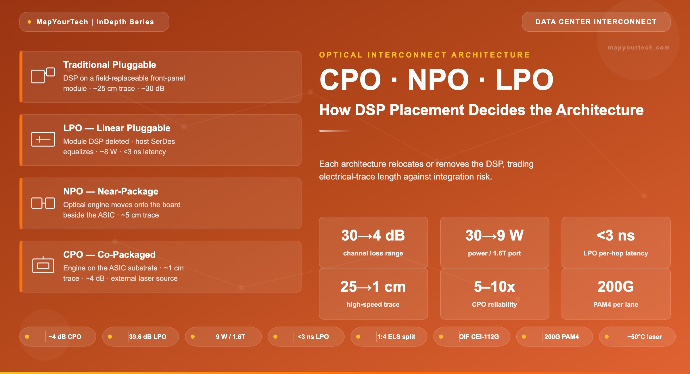
CPO, NPO, LPO: How DSP Placement Decides the Architecture
Four optical interconnect architectures, one variable that decides them all: where the signal-conditioning silicon sits, and how far its electrical output has to travel before it becomes light.
1. Introduction
A 1.6 Tb/s switch ASIC drives 256 differential lanes at 200 Gb/s PAM4. Each lane leaves the die, crosses the package, traverses tens of centimetres of printed circuit board, passes through a connector, and finally reaches a pluggable module at the front panel. By the time a 200 Gb/s signal completes that trip on a conventional board, it has lost roughly 30 dB of amplitude and arrived as a smeared, intersymbol-interference-laden waveform that no analog receiver could recover. That is the problem the digital signal processor solves, and the reason every transceiver shipped at 400 Gb/s and 800 Gb/s carries one.
The DSP is also the largest single power consumer in the module. Of the roughly 30 W a 1.6T pluggable draws, Nvidia attributes about 20 W to the DSP and 10 W to the laser. Multiply by hundreds of ports per switch and tens of thousands of switches per AI cluster, and DSP power becomes a megawatt-class line item that scales linearly with bandwidth. The industry's response has been to ask a simple question with four different answers: if the electrical path is what forces the DSP to be so capable, what happens if you shorten the path?
Each architecture in this article answers that question by relocating or removing the DSP. Traditional pluggable optics keep a full DSP on the module. Linear pluggable optics (LPO) delete the module DSP and lean on the host ASIC. Near-packaged optics (NPO) move the optical engine off the front panel to a position beside the ASIC. Co-packaged optics (CPO) place the optical engine on the ASIC substrate itself. The DSP does not change function across these four — it always recovers the signal — but where it lives, and how far its electrical output must travel, changes everything downstream: power, density, latency, serviceability, and who owns the supply chain.
This article maps all four placements against the physics that motivates them and the deployment reality of 2026. For a broader view of how these form factors fit the wider transceiver market, the MapYourTech analysis of optical pluggable technology trends and future outlook provides useful context. The scope here is intra-data-center and scale-up interconnect at 200 Gb/s per lane, where the placement question is being decided in production right now.
2. The DSP, and Why Its Position Is the Design Variable
The transceiver DSP performs four jobs that together let a clean digital lane survive a hostile electrical and optical channel. It retimes the signal with clock and data recovery, recovering symbol timing from the incoming waveform. It equalizes, applying feed-forward and decision-feedback filters that reverse the channel's frequency-dependent loss. It encodes and decodes forward error correction, typically KP4 Reed-Solomon at these rates, trading a few percent of overhead for orders of magnitude of bit-error-rate improvement. And it re-modulates, driving the laser or modulator with a conditioned electrical signal. The signal-conditioning load on the DSP is set almost entirely by how degraded the waveform is when it arrives.
That degradation comes mostly from the electrical channel, not the optics. A 200 Gb/s PAM4 lane occupies a Nyquist frequency near 28 GHz, and copper loss rises steeply with both frequency and distance. The relationship that governs how hard the DSP must work is the channel insertion loss budget the SerDes can tolerate.
Read the Full Analysis with Premium
The remaining 88% of this article — the design numbers, trade-offs and field guidance — is part of MapYourTech Premium, along with the full premium library, courses and professional tools.
You May Also Like
-
Free
-
September 4, 2026
-
Premium
-
September 4, 2026
-
Premium
-
September 4, 2026