 MapYourTech | InDepth Series
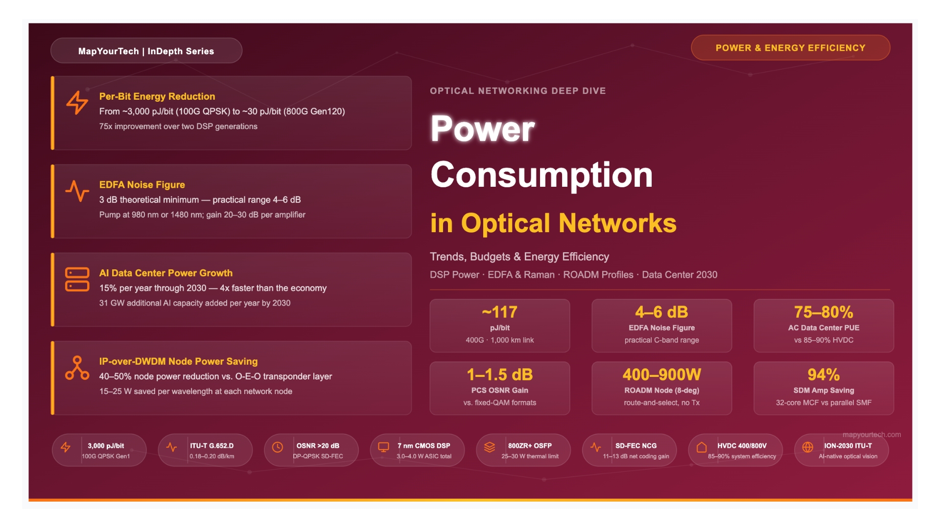
Power Consumption in Optical Networks:
Trends, Budgets, and Energy Efficiency
A research-grade treatment of per-bit energy trends for coherent DSPs, EDFA and Raman pump power, ROADM power profiles, data center power outlook through 2030, and the engineering approaches that determine whether optical infrastructure keeps pace with a world running on AI.
Introduction
Energy is the defining constraint of modern optical networking. Not bandwidth. Not latency. Not reach. Energy. As the industry crossed the threshold into the era of terabit coherent transport and AI-driven hyperscale data centers, the question that once dominated engineering reviews — "can we carry enough bits?" — has been quietly replaced by a more consequential one: "can we power the infrastructure to carry them?"
The numbers make the urgency plain. Data center electricity consumption is projected to grow at approximately 15% per year through 2030, more than four times faster than the broader economy, according to projections presented at OFC 2026. McKinsey & Company estimated in April 2025 that the period from 2025 to 2030 would require roughly $6.6 trillion in data center investment, with $5.2 trillion of that driven by AI and Machine Learning workloads. Of that staggering sum, approximately $1.5 trillion goes toward power infrastructure alone — generators, transformers, rectifiers, distribution units — before a single optical transceiver or amplifier is accounted for.
Optical transport sits at the center of this challenge from two directions simultaneously. On one side, optical networks must carry the explosive traffic generated by AI training and inference across data center interconnects, metro rings, and long-haul backbone links — all at lower cost and lower power per bit than the generation before. On the other side, the optical infrastructure inside and between data centers is itself a significant power consumer, with coherent Digital Signal Processing (DSP) ASICs, Erbium-Doped Fiber Amplifiers (EDFAs), Raman pump lasers, and Reconfigurable Optical Add-Drop Multiplexers (ROADMs) drawing hundreds of watts per node, collectively reaching tens of megawatts across a large network.
This article provides a comprehensive, quantitative treatment of power consumption across the full optical transport stack. It covers the theoretical foundations that govern energy efficiency, traces the per-bit energy trajectory of coherent DSP from 40 nm to sub-3 nm CMOS geometries, examines the pump power economics of EDFA and Raman amplification, profiles the power draw of ROADM nodes across generations, and situates all of this within the broader data center power outlook running to 2030. Engineering approaches to energy optimization — from probabilistic constellation shaping to pluggable optics to high-voltage DC power distribution — are treated with the analytical depth that design engineers and network architects require.
Historical Context and Literature Baseline
2.1 From 10G to 800G: The Per-Bit Energy Journey
The history of optical networking is, in large part, a story of relentless per-bit cost reduction — and nowhere is that more visible than in energy consumption. In the early 2000s, a 10 Gbps wavelength on a SONET/SDH long-haul link consumed on the order of 10–15 watts per transceiver, yielding a per-bit figure of roughly 1–1.5 W/Gbps, or 1,000–1,500 pJ/bit. The signal processing was limited — direct detection with fixed dispersion compensation modules — but the component power density was high relative to the capacity delivered.
The introduction of coherent detection and DSP-based impairment compensation after 2008 initially increased total transceiver power. Early 100G PM-QPSK (Polarization-Multiplexed Quadrature Phase Shift Keying) transceivers in CFP form factors consumed 24 to 32 watts — significantly more than their 10G predecessors per device, though now delivering 10× the capacity. This brought the per-bit figure down to approximately 2.5–3 W/Gbps, or 2,500–3,000 pJ/bit.
The subsequent decade saw each new generation of coherent DSP, manufactured in successively smaller CMOS process nodes, deliver substantial reductions in per-bit energy. The progression from 40 nm CMOS (first-generation coherent DSPs) through 28 nm, 16 nm, and 7 nm nodes tracked closely with Moore's law scaling predictions for digital logic power. Each process shrink delivered roughly 30–50% reduction in DSP power for equivalent computational workload, though the workload itself expanded with higher modulation formats, wider baud rates, and more sophisticated forward error correction algorithms.
Figure 1: Per-Bit Energy Consumption — Coherent Transceiver Generations
Figure 1: Approximate per-bit energy consumption (pJ/bit) across coherent transceiver generations. Values reflect typical deployed implementations; actual figures vary by vendor and reach configuration. Sources: project references and published literature.
By the 400G generation, manufactured on 7 nm CMOS, coherent transceivers in CFP2-ACO form factors consumed around 30 watts for the DSP ASIC portion alone — but at 400 Gbps capacity, this translates to approximately 0.075 W/Gbps or 75 pJ/bit, roughly a 30× improvement over first-generation 100G systems. The 800G generation, entering volume deployment in 2025–2026 using advanced 5 nm and 4 nm CMOS processes, targets the region of 25–40 pJ/bit in high-performance embedded implementations and somewhat higher in pluggable OSFP modules constrained by thermal envelopes.
2.2 CMOS Scaling and the DSP Dividend
The dominant driver of per-bit energy improvement in coherent transport has been CMOS process scaling. The progression from 40 nm to 28 nm, 16 nm, 7 nm, and now 4–3 nm nodes has delivered consistent reductions in switching energy per transistor, allowing DSP designers to execute more complex algorithms within the same or lower power envelope. The relationship follows Dennard's scaling rules for digital logic: as feature size shrinks by a factor of two, switching capacitance drops proportionally, and power supply voltage can be reduced, yielding a quadratic improvement in energy per operation in the ideal case.
In practice, the benefits are somewhat lower than the theoretical ideal because the algorithms themselves have grown significantly more demanding. Coherent DSPs now implement soft-decision forward error correction (SD-FEC) with net coding gains of 11–13 dB, chromatic dispersion compensation spanning thousands of kilometers worth of accumulated dispersion, polarization-mode dispersion tracking and equalization, nonlinear compensation algorithms that model fiber Kerr effects, and probabilistic constellation shaping that requires additional arithmetic to compute non-uniform symbol probabilities. Each new generation adds computational layers that partially offset the process dividend.
CMOS Process and DSP Power
Published data from Cisco's vertical integration roadmap (presented at industry events in 2025) shows the CMOS node progression for coherent DSPs: 40 nm → 28 nm → 16 nm → 7 nm → 4/3 nm → 2 nm (roadmap). Each generation also advanced the modulation format capability: QPSK → QPSK → 16QAM → 16QAM with PCS → PCS/advanced shaping → PCS at higher baud rates. The implication is that the industry has been able to add substantial DSP capability while reducing per-bit power — but the absolute power of the DSP chip itself has sometimes increased between generations as baud rate and algorithm complexity grew faster than the process efficiency gain.
2.3 The AI Inflection: Why 2026 Is Different
The period from approximately 2022 to 2026 represents a qualitative shift in the power dynamics of optical networking, driven by the explosive growth of AI workloads. This is not merely a steeper point on a previously established growth curve. The scale, concentration, and thermal density of AI data centers differ categorically from conventional cloud workloads, and these differences cascade into the optical interconnect requirements in ways that make power efficiency both more difficult to achieve and more commercially urgent.
AI training clusters — operating at scales of tens of thousands of accelerator chips with all-to-all communication requirements — generate interconnect traffic patterns and bandwidth concentrations that conventional WAN-optimized optical networks were not designed for. The back-end fabric connecting GPU clusters must simultaneously achieve extremely high bandwidth density, very low latency, and low power per port to stay within the thermal envelope of the rack. The result is a bifurcation in the optical interconnect market: the back-end fabric pulling toward very short-reach, ultra-low-power intensity-modulated direct-detection (IM-DD) optics; and the front-end wide-area connectivity pulling toward pluggable coherent optics at 400G, 800G, and, from 2026 onward, 1.6T, where power efficiency is measured in watts per port.
AI heat densities have also begun to outpace the capacity of air cooling, forcing transitions to liquid cooling architectures that fundamentally alter data center power distribution design. The shift toward liquid cooling could push global data center water consumption to approximately 450 million gallons per day by 2030, according to projections presented at OFC 2026 — equivalent to the daily water needs of five million people. This is not an optical networking problem per se, but it creates the infrastructure context within which optical engineers are now operating: every watt saved in a transceiver or amplifier directly reduces the cooling burden on an already stressed thermal management system.
Read the Full Analysis with Premium
The remaining 88% of this article — the design numbers, trade-offs and field guidance — is part of MapYourTech Premium, along with the full premium library, courses and professional tools.