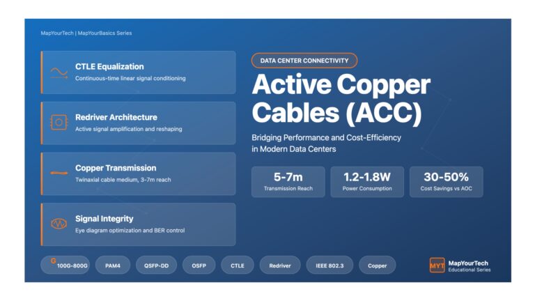
Active Copper Cables (ACC): Comprehensive Technical Guide | MapYourTech Active Copper Cables (ACC) Comprehensive Technical Guide to Modern Data Center...
Active Optical Cables (AOC): Complete Educational Guide Active Optical Cables (AOC): Complete Educational Guide Master the fundamentals, architecture, and applications...
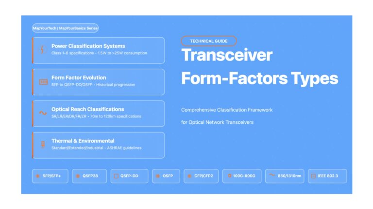
Comprehensive Guide to Transceiver Class Types in Optical Networking Comprehensive Guide to Transceiver Form-Factors Types in Optical Networking A Technical...