Author

MapYourTech

Browsing
Share and Explore the Tech Inside You!!!

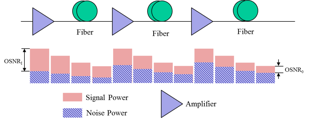
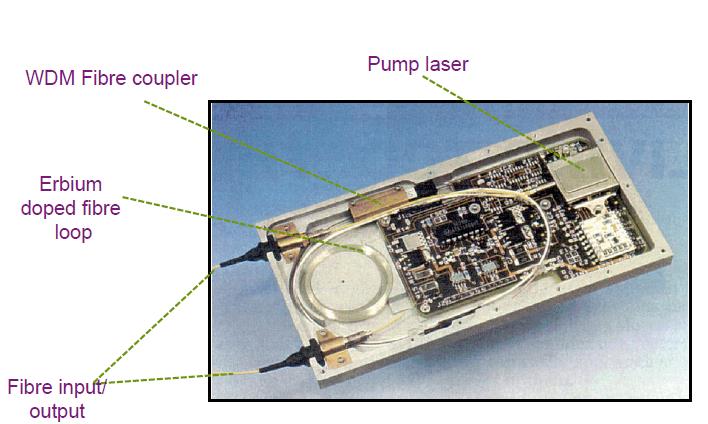
The maximum number of erbium-doped fiber amplifiers (EDFAs) in a fiber chain is about four to  six.
edfa


Explanation 

The rule is based on the following rationales:

1. About 80 km exists between each in-line EDFA, because this is the approximate distance at which the signal needs to be amplified.

2. One booster is used after the transmitter.

3. One preamplifier is used before the receiver.

4. Approximately 400 km is used before an amplified spontaneous emission (ASE) has approached the signal (resulting in a loss of optical signal-to-noise ratio [OSNR]) and regeneration needs to be used.

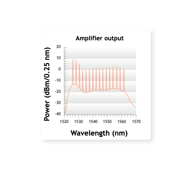
An EDFA amplifies all the wavelengths and modulated as well as unmodulated light. Thus, every time it is used, the noise floor from stimulated emissions rises. Since the amplification actually adds power to each band (rather than multiplying it), the signal-to-noise ratio is decreased at each amplification. EDFAs also work only on the C and L bands and are typically pumped with a 980- or 1480-nm laser to excite the erbium electrons. About 100 m of fiber is needed for a 30-dB gain, but the gain curve doesn’t have a flat distribution, so a filter is usually included to ensure equal gains across the C and L bands.

For example, assume that the modulated power was 0.5 mW, and the noise from stimulated emission was 0.01 mW. The signal-to-noise ratio is 0.5/0.01 or 50. If an EDFA adds a 0.5 mW to both the modulated signal and the noise, then the modulated signal becomes 1 mW, and the noise becomes 0.501 mW, and the SNR is reduced to 2. After many amplifications,even if the total power is high, the optical signal-to-noise ratio becomes too low. This typically occurs after four to six amplifications.

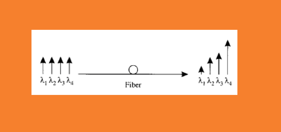
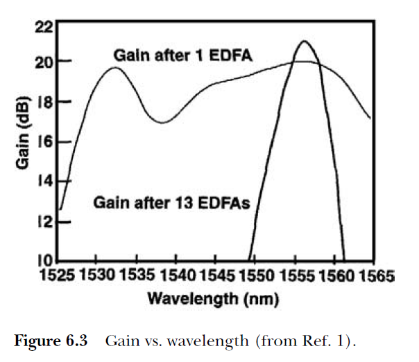
Another reason to limit the number of chained EDFAs is the nonuniform nature of the gain. Generally, the gain peaks at 1555 nm and falls off on each side, and it is a function of the inversion of Er+3. When a large number of EDFAs are cascaded, the sloped of the gain becomes multiplied and sharp, as indicated in Fig. 6.3. This results is too little gain-bandwidth for a system. To help alleviate this effect, a gain flattening device often is used, such as a Mach–Zehnder or a long-period grating filter.


Reference

1. A. Willner and Y. Xie, “Wavelength Domain Multiplexed (WDM) Fiber-optic Communications Networks,” in Handbook of Optics, Vol. 4., M. Bass, Ed.,McGraw-Hill, New York, pp. 13–19, 2001.

2.http://www.pandacomdirekt.com/en/technologies/wdm/optical-amplifiers.html

3.http://blog.cubeoptics.com/index.php/2015/03/what-edfa-a-noise-source

Source: Optical Communications Rules of Thumb

Note:I have heard many times among optical folks discussing  maximum number of amplifiers in a link;so thought of posting this.

Few analogies proving the subject:-

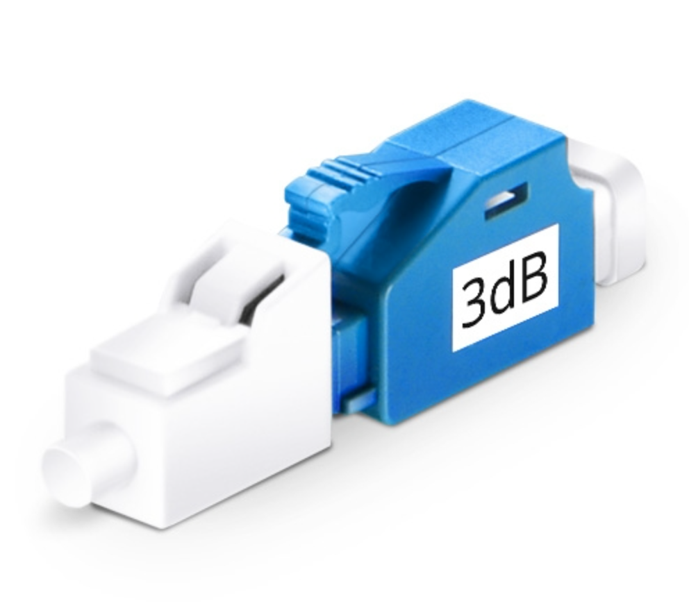
  • If the distance is to short and the attenuator is too close to the transmitter, the reflected light off the attenuator will be directed back towards the Tx laser. Which will also blow your transmitter.so we place it at Rx.
  • Also keeping attenuator at Rx will attenuate the noise along with the signal.
  • The most important reason for putting them on the RX side is that you are protecting that which needs to be protected – the receiver in your optics. This way you know that you’re not going to potentially blow the receiver in your optics by plugging in too large a signal because you assumed there was an attenuator on the TX at the far end, and there wasn’t.
  • It’s more convenient to test the receiver power before and after attenuation or while adjusting it with your power meter at the receiver, plus any reflectance will be attenuated on its path back to the source.


Keynote on Using Attenuators With Fiber Optic Data Links


BER

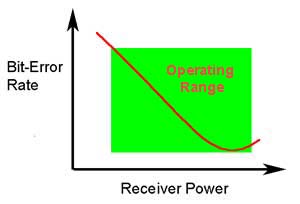
The ability of any fiber optic system to transmit data ultimately depends on the optical power at the receiver as shown above, which shows the data link bit error rate as a function of optical power at the receiver. (BER is the inverse of signal-to-noise ratio, e.g. high BER means poor signal to noise ratio.)  Either too little or too much power will cause high bit error rates.

Too much power, and the receiver amplifier saturates, too little and noise becomes a problem as it interferes with the signal. This receiver power depends on two basic factors: how much power is launched into the fiber by the transmitter and how much is lost by attenuation in the optical fiber cable plant that connects the transmitter and receiver.

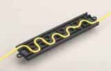
If the power is too high as it often is in short singlemode systems with laser transmitters, you can reduce receiver power with an attenuator. Attenuators can be made by introducing an end gap between two fibers (gap loss), angular or lateral misalignment, poor fusion splicing (deliberately), inserting a neutral density filter or even stressing the fiber (usually by a serpentine holder or a mandrel wrap). Attenuators are available in models with variable attenuation or with fixed values from a few dB to 20 dB or more.

gap loss attenuators
Gap-loss attenuators for multimode fiber
serpentine attenuator
Serpentine attenuators for singlemode fiber
Generally, multimode systems do not need attenuators. Multimode sources, even VCSELs, rarely have enough power output to saturate receivers. Singlemode systems, especially short links, often have too much power and need attenuators.

For a singlemode applications, especially analog CATV systems, the most important specification, after the correct loss value, is return loss or reflectance! Many types of attenuators (especially gap loss types) suffer from high reflectance, so they can adversely affect transmitters just like highly reflective connectors.

attenuators in fiber optic data link

Choose a type of attenuator with good reflectance specifications and always install the attenuator ( X in the drawing) as shown at the receiver end of the link. This is because it’s more convenient to test the receiver power before and after attenuation or while adjusting it with your power meter at the receiver, plus any reflectance will be attenuated on its path back to the source.

testing attenuated power at receiver
Test the system power with the transmitter turned on and the attenuator installed at the receiver using a fiber optic power meter set to the system operating wavelength. Check to see the power is within the specified range for the receiver.

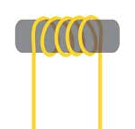
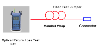
If the appropriate attenuator is not available, simply coil some patchcord around a pencil while measuring power with your fiber optic power meter, adding turns until the power is in the right range. Tape the coil and your system should work. This type of attenuator has no reflectance and is very low cost! The fiber/cable manufacturers may worry about the relaibility of a cable subjected to such a small bend radius. You should probably replace it with another type of attenuator at some point, however.

singlemode wrap attenuator
Singlemode attenuator made by wrapping fiber or simplex cable around a small mandrel. This will not work well with bend-insensitive fiber.

ref:http://www.thefoa.org/tech/ref/appln/attenuators.html

Power Change during add/remove of channels on filters

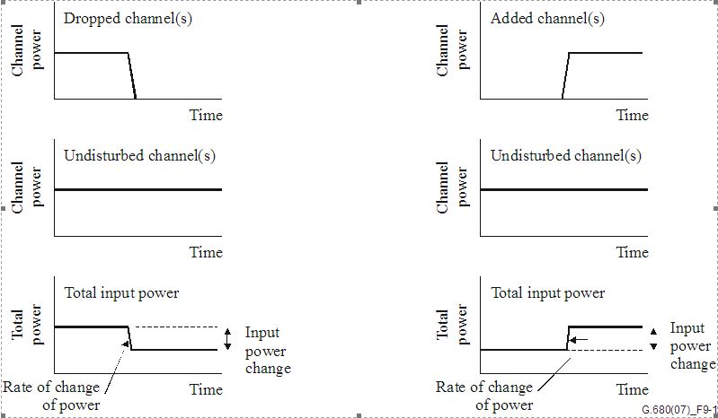
The power change can be quantified as the ratio between the number of channels at the reference point after the channels are added or dropped and the number of channels at that reference point previously. We can consider composite power here and each channel at same optical power in dBm.

So whenever we add or delete number of channels from a MUX/DEMUX/FILTER/WSS following equations define the new changed power.

For the case when channels are added (as illustrated on the right side of Figure 1 ):

where:

A   is the number of added channels

U   is the number of undisturbed channels

For the case when channels are dropped (as illustrated on the left side of Figure 1):


where:

D   is the number of dropped channels

U   is the number of undisturbed channels


 Figure 1

For example:

–           adding 7 channels with one channel undisturbed gives a power change of +9 dB;

–           dropping 7 channels with one channel undisturbed gives a power change of –9 dB;

–           adding 31 channels with one channel undisturbed gives a power change of +15 dB;

–           dropping 31 channels with one channel undisturbed gives a power change of –15 dB;

refer ITU-T G.680 for further study.

Items HD-FEC SD-FEC
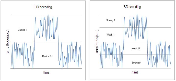
Definition Decoding based on hard-bits(the output is quantized only to two levels) is called the “HD(hard-decision) decoding”, where each bit is considered definitely one or zero. Decoding based on soft-bits(the output is quantized to more than two levels) is called the “SD(soft-decision) decoding”, where not only one or zero decision but also confidence information for the decision are provided.
Application Generally for non-coherent detection optical systems, e.g.,  10 Gbit/s, 40 Gbit/s, also for some coherent detection optical systems with higher OSNR coherent detection optical systems, e.g.,  100 Gbit/s,400 Gbit/s.
Electronics Requirement ADC(Analogue-to-Digital Converter) is not necessary in the receiver. ADC is required in the receiver to provide soft information, e.g.,  coherent detection optical systems.
specification general FEC per [ITU-T G.975];super FEC per [ITU-T G.975.1]. vendor specific
typical scheme Concatenated RS/BCH LDPC(Low density parity check),TPC(Turbo product code)
complexity medium high
redundancy ratio generally 7% around 20%
NCG about 5.6 dB for general FEC;>8.0 dB for super FEC. >10.0 dB
 Example(If you asked your friend about traffic jam status on roads and he replies) maybe fully jammed or free  50-50  but I found othe way free or less traffic

What is a OTDR ?

Optical Time Domain Reflectometer – also known as an OTDR, is a hardware device used for measurement of the elapsed time and intensity of light reflected on optical fiber.

How it works?

The reflectometer can compute the distance to problems on the fiber such as attenuation and breaks, making it a useful tool in optical network troubleshooting.

The intensity of the return pulses is measured and integrated as a function of time, and is plotted as a function of fiber length.

What is a COTDR?

Coherent Optical Time Domain Reflectometer – also known as a COTDR, An instrument that is used to perform out of service backscattered light measurements on optically amplified line systems.

How it works?

A fiber pair is tested by launching a test signal into the out going fiber and receiving the scattered light on the in-coming fiber.  Light scattered in the transmission fiber is coupled to the incoming fiber in the loop-back couplers in each amplifier pair in a repeater.


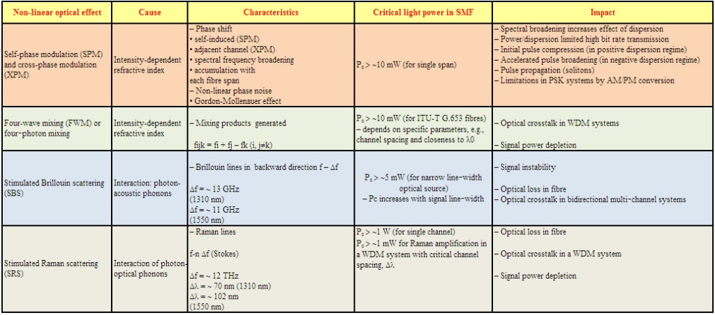
Non-linear interactions between the signal and the silica fibre transmission medium begin to appear as optical signal powers are increased to achieve longer span lengths at high bit rates. Consequently, non-linear fibre behaviour has emerged as an important consideration both in high capacity systems and in long unregenerated routes. These non-linearities can be generally categorized as either scattering effects (stimulated Brillouin scattering and stimulated Raman scattering) or effects related to the fibre’s intensity dependent index of refraction (self-phase modulation, cross-phase modulation, modulation instability, soliton formation and four-wave mixing). A variety of parameters influence the severity of these non-linear effects, including line code (modulation format), transmission rate, fibre dispersion characteristics, the effective area and non-linear refractive index of the fibre, the number and spacing of channels in multiple channel systems, overall unregenerated system length, as well as signal intensity and source line-width. Since the implementation of transmission systems with higher bit rates than 10 Gbit/s and alternative line codes (modulation formats) than NRZ-ASK or RZ-ASK, described in [b-ITU-T G-Sup.39], non‑linear fibre effects previously not considered can have a significant influence, e.g., intra‑channel cross-phase modulation (IXPM), intra-channel four-wave mixing (IFWM) and non‑linear phase noise (NPN).


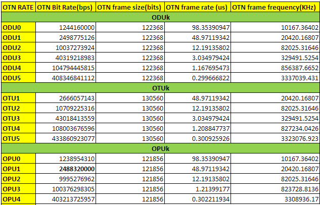
**Multiplicative factor is just a simple math :eg. for ODU1/OPU1=3824/3808={(239*16)/(238*16)}

Here value of multiplication factor will give the number of times for rise in the frame size after adding header/overhead.

Example:let consider y=(x+delta[x])/xIn terms of OTN frame here delta[x] is increment of Overhead.

As we are using Reed Soloman(255,239) i.e we are dividing 4080bytes in sixteen frames (The forward error correction for the OTU-k uses 16-byte interleaved codecs using a Reed- Solomon S(255,239) code. The RS(255,239) code operates on byte symbols.).Hence 4080/16=255.

Try to understand using OTN frames now. I have tried to make it legible.

As we know that OPU1 payload rate= 2.488 Gbps (OC48/STM16) and is  frame size is 4*3808 as below.

*After adding OPU1 and ODU1 16 bytes overhead: Frames could be fragmented into following number of chunks.

3808/16 = 238, (3808+16)/16 = 239

So, ODU1 rate: 2.488 x 239/238** ~ 2.499Gbps

*Now after adding  FEC bytes

OTU1 rate: ODU1 x 255/239 = 2.488 x 239/238 x 255/239

=2.488 x 255/238 ~2.667Gbps


Now let’s have a small discussion over different multiplier and divisor scenarios that will make it clearer to understand.

We know that an OTU frame 4 * 4080 bytes (= 255 * 16 * 4)

OPU representing the Payload (3824-16) * 4 * 4 = 3808 bytes (= 238 * 16 * 4) .

OPU1 is exactly the rate of STM-16.

Now,

ODU1 = (3824/3808) * OPU1 = ((16 * 239) / (238 16 *)) * OPU1 = (239/238) * STM-16

OTU1 = (4080/3808) * OPU1 = ((255 * 16) / (238 * 16)) * OPU1 = (255/238) * STM-16


OPU2 contains 16 * 4 = 64 bytes of fixed stuff (FS) added to the 1905 to 1920 .

OPU2 * ((238 * 16 * 4-16 * 4) / (238 * 16 * 4)) = STM-64 rate

OPU2 = 238 / (238-1) * STM-64 = 238/237* STM-64 rate

ODU2 = (239/237) * STM-64 rate ,

similarly


OTU2 = ( 255/237) * STM-64 rate

OPU3 Including 2 * 16 * 4 = 128 fixed stuff (FS) bytes added to the 1265 ~ 1280 and 2545 ~ 2560

OPU3 * ((238 * 16 * 4-2 * 16 * 4) / (238 * 16 * 4)) = rate of STM-256

OPU3 = 238 / (238-2) * STM-256 = 238/236 * STM-256

ODU3 = (239 / 236) * STM-256

OTU3 = (255/236) * STM-256

The OTU4 was required to transport ten ODU2e signals, which have a non-SDH based clock frequency as basis. The OTU4 clock should be based on the same SDH clock as the OTU1, OTU2 and OTU3 and not on the 10GBASE-R clock, which determines the ODU2e frequency. An exercise was performed to determine the necessary divider in the factor 255/divider, and the value 227 was found to meet the requirements (factor 255/227). Note that this first analysis has indicated that a future 400 Gbit/s OTU5 could be created using a factor 255/226 and a 1 Tbit/s OTU6 using a factor 255/225.
Optical power tolerance: It refers to the tolerable limit of input optical power, which is the range from sensitivity to overload point.

Optical power requirement: If refers to the requirement on input optical power, realized by adjusting the system (such as adjustable attenuator, fix attenuator, optical amplifier).


Optical power margin: It refers to an acceptable extra range of optical power. For example, “–5/ + 3 dB” requirement is actually a margin requirement.

When the bit error occurs to the system, generally the OSNR at the transmit end is well and the fault is well hidden.
Decrease the optical power at the transmit end at that time. If the number of bit errors decreases at the transmit end, the problem is non-linear problem.
If the number of bit errors increases at the transmit end, the problem is the OSNR degrade problem. 


General Causes of Bit Errors

  •  Performance degrade of key boards
  • Abnormal optical power
  • Signal-to-noise ratio decrease
  • Non-linear factor
  • Dispersion (chromatic dispersion/PMD) factor
  • Optical reflection
  • External factors (fiber, fiber jumper, power supply, environment and others)

The main advantages and drawbacks of EDFAs are as follows.
Advantages

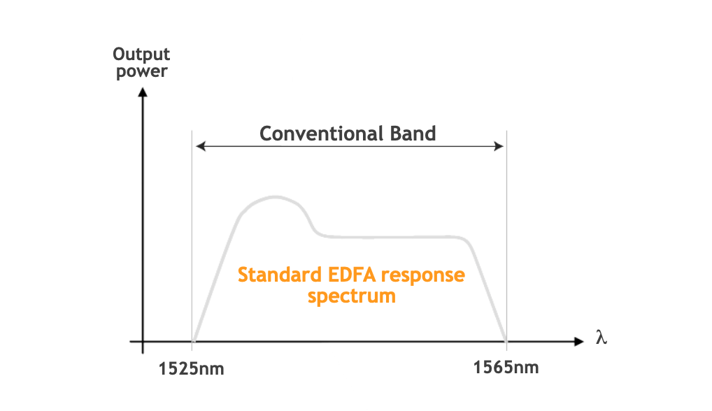
  • Commercially available in C band (1,530 to 1,565 nm) and L band (1,560 to 1,605) and up to  84-nm range at the laboratory stage.
  • Excellent coupling: The amplifier medium is an SM fiber;
  • Insensitivity to light polarization state;
  • Low sensitivity to temperature;
  • High gain: > 30 dB with gain flatness < ±0.8 dB and < ±0.5 dB in C and L band, respectively, in the scientific literature and in the manufacturer documentation
  • Low noise figure: 4.5 to 6 dB
  • No distortion at high bit rates;
  • Simultaneous amplification of wavelength division multiplexed signals;
  • Immunity to crosstalk among wavelength multiplexed channels (to a large extent)

Drawbacks

  • Pump laser necessary;
  • Difficult to integrate with other components;
  • Need to use a gain equalizer for multistage amplification;
  • Dropping channels can give rise to errors in surviving channels:dynamic control of amplifiers is  necessary.

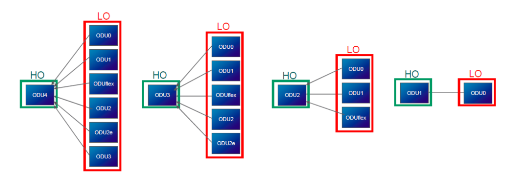
A Lower Order-ODU or LO-ODU is an ODUk, whose OPUk transports a inside mapped client.


An Higher Order-ODU or HO-ODU is an ODUk, whose OPUk transports an inside multiplexed ODUj.
LO-ODU and HO-ODU have the same structure but with different clients.
The LO-ODU is either mapped into the associated OTUk or multiplexed into an HO-ODU.
The HO-ODU is mapped into the associated OTUk.
Please notice that, HO-ODUj multiplexed into HO-ODUk is an undesired hierarchy in one domain.

The ITU standards define a “suspect internal flag” which should indicate if the data contained within a register is ‘suspect’ (conditions defined in Q.822). This is more frequently referred to as the IDF (Invalid Data Flag).

PM is bounded by strict data collection  rules as defined in standards. When the collection of PM parameters is affected then  PM system labels the collection of data as suspect with an Invalid Data Flag (IDF). For the sake of identification; some unique flag  is shown next to corresponding counter.

The purpose of the flag is to indicate when the data in the PM bin may not be complete or may have been affected such that the data is not completely reliable. The IDF does not mean the software is contingent.

Some of the common reasons  for setting the IDF include:

  • a collection time period that does not start within +/- 1 second of the nominal collection window start time.
  • a time interval that is inaccurate by +/- 10 seconds (or more)
  • the current time period changes by +/- 10 seconds (or more)
  • a restart (System Controller restarts will wipe out all history data and cause time fluctuations at line/client module;  a module restart will wipe out the current counts)
  • a PM bin is cleared manually
  • a hardware failure prevents PM from properly collecting a full period of PM data (PM clock failure)
  • a protection switch has caused a change of payload on a protection channel.
  • a payload reconfiguration has occurred (similar to above but not restricted to protection switches).
  • an System Controller archive failure has occurred, preventing history data from being collected from the line/client  cards
  • protection mode is switched from non-revertive to revertive (affects PSD only)
  • a protection switch clear indication is received when no raise was indicated
  • laser device failure (affects physical PMs)
  • loss of signal (affects receive – OPRx, IQ – physical PMs only)
  • Control Plane is booted less than 15 min period for 15-min interval and less than 24 hour period for 24-hour interval.

Suspect interval is determined by comparing nSamples to nTotalSamples on a counter PM. If nSamples is not equal to nTotalSamples then this period can be marked as suspect. 

If any 15 minute is marked as suspect or reporting for that day interval is not started at midnight then it should flag that 24 Hr as suspect.

Some of the common examples are:

  • Interface type is changed to another compatible interface (10G SR interface replaced by 10G DWDM interface),
  • Line type is changed from SONET to SDH,
  • Equipment failures are detected and those failures inhibit the accumulation of PM.
  • Transitions to/from the ‘locked’ state.
  • The System shall mark a given accumulation period invalid when the facility object is created or deleted during the interval.
  • Node time is changed.

A short discussion on 980nm and 1480nm pump based EDFA

Introduction

The 980nm pump needs three energy level for radiation while 1480nm pumps can excite the ions directly to the metastable level .edfa

(a) Energy level scheme of ground and first two excited states of Er ions in a silica matrix. The sublevel splitting and the lengths of arrows representing absorption and emission transitions are not drawn to scale. In the case of the 4 I11/2 state, s is the lifetime for nonradiative decay to the I13/2 first excited state and ssp is the spontaneous lifetime of the 4 I13/2 first excited state. (b) Absorption coefficient, a, and emission coefficient, g*, spectra for a typical aluminum co-doped EDF.

The most important feature of the level scheme is that the transition energy between the I15/2 ground state and the I13/2 first excited state corresponds to photon wavelengths (approximately 1530 to 1560 nm) for which the attenuation in silica fibers is lowest. Amplification is achieved by creating an inversion by pumping atoms into the first excited state, typically using either 980 nm or 1480 nm diode lasers. Because of the superior noise figure they provide and their superior wall plug efficiency, most EDFAs are built using 980 nm pump diodes. 1480 nm pump diodes are still often used in L-band EDFAs although here, too, 980 nm pumps are becoming more widely used.

Though pumping with 1480 nm is used and has an optical power conversion efficiency which is higher than that for 980 nm pumping, the latter is preferred because of the following advantages it has over 1480 nm pumping.

  • It provides a wider separation between the laser wavelength and pump wavelength.
  • 980 nm pumping gives less noise than 1480nm.
  • Unlike 1480 nm pumping, 980 nm pumping cannot stimulate back transition to the ground state.
  • 980 nm pumping also gives a higher signal gain, the maximum gain coefficient being 11 dB/mW against 6.3 dB/mW for the 1.48
  • The reason for better performance of 980 nm pumping over the 1.48 m pumping is related to the fact that the former has a narrower absorption spectrum.
  • The inversion factor almost becomes 1 in case of 980 nm pumping whereas for 1480 nm pumping the best one gets is about 1.6.
  • Quantum mechanics puts a lower limit of 3 dB to the optical noise figure at high optical gain. 980 nm pimping provides a value of 3.1 dB, close to the quantum limit whereas 1.48  pumping gives a value of 4.2 dB.
  • 1480nm pump needs more electrical power compare to 980nm.

Application

The 980 nm pumps EDFA’s are widely used in terrestrial systems while 1480nm pumps are used as Remote Optically Pumped Amplifiers (ROPA) in subsea links where it is difficult to put amplifiers.For submarine systems, remote pumping can be used in order not to have to electrically feed the amplifiers and remove electronic parts.Nowadays ,this is used in pumping up to 200km.

The erbium-doped fiber can be activated by a pump wavelength of 980 or 1480 nm but only the second one is used in repeaterless systems due to the lower fiber loss at 1.48 mm with respect to the loss at 0.98 mm. This allows the distance between the terminal and the remote amplifier to be increased.

In a typical configuration, the ROPA is comprised of a simple short length of erbium doped fiber in the transmission line placed a few tens of kilometers before a shore terminal or a conventional in-line EDFA. The remote EDF is backward pumped by a 1480 nm laser, from the terminal or in-line EDFA, thus providing signal gain

Vendors

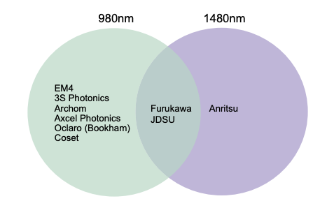
Following are the vendors that manufactures 980nm and 1480nm EDFAs

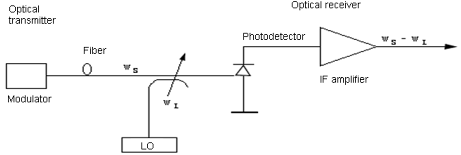
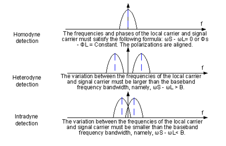
As we know that either homodyne or heterodyne detection can be used to convert the received optical signal into an electrical form. In the case of homodyne detection, the optical signal is demodulated directly to the baseband. Although simple in concept, homodyne detection is difficult to implement in practice, as it requires a local oscillator whose frequency matches the carrier frequency exactly and whose  phase is locked to the incoming signal. Such a demodulation scheme is called synchronous and is essential for homodyne detection. Although optical phase-locked loops have been developed for this purpose, their use is complicated in practice.

Heterodyne detection simplifies the receiver design, as neither optical phase locking nor frequency matching of the local oscillator is required. However, the electrical signal  oscillates rapidly at microwave frequencies and must be demodulated from the IF bandto the baseband using techniques similar to those developed for microwave communication systems. Demodulation can be carried out either synchronously or asynchronously. Asynchronous demodulation is also called incoherent in the radio communication literature. In the optical communication literature, the term coherent detection is used in a wider sense.

A lightwave system is called coherent as long as it uses a local oscillator irrespective of the demodulation technique used to convert the IF signal to baseband frequencies.

*In case of homodyne coherent-detection technique, the local-oscillator frequency is selected to coincide with the signal-carrier frequency.

*In case of heterodyne detection the local-oscillator frequency  is chosen to differ from the signal-carrier frequency.

What Is Coherent Communication?

Definition of coherent light

A coherent light consists of two light waves that:

1) Have the same oscillation direction.

2) Have the same oscillation frequency.

3) Have the same phase or maintain a constant phase relationship with each other. Two coherent light waves produce interference within the area where they meet.

Principles of Coherent Communication

Coherent communication technologies mainly include coherent modulation and coherent detection.

Coherent modulation uses the signals that are propagated to change the frequencies, phases, and amplitudes of optical carriers. (Intensity modulation only changes the strength of light.)

Modulation detection mixes the laser light generated by a local oscillator (LO) with the incoming signal light using an optical hybrid to produce an IF signal that maintains the constant frequency, phase, and amplitude relationships with the signal light.


The motivation behind using the coherent communication techniques is two-fold.

First, the receiver sensitivity can be improved by up to 20 dB compared with that of IM/DD systems.

Second, the use of coherent detection may allow a more efficient use of fiber bandwidth by increasing the spectral efficiency of WDM systems

coherent
#coherent

In a non-coherent WDM system, each optical channel on the line side uses only one binary channel to carry service information. The service transmission rate on each optical channel is called bit rate while the binary channel rate is called baud rateIn this sense, the baud rate was equal to the bit rate. The spectral width of an optical signal is determined by the baud rate. Specifically, the spectral width is linearly proportional to the baud rate, which means a higher baud rate generates a larger spectral width.

  • Baud (pronounced as /bɔ:d/ and abbreviated as “Bd”) is the unit for representing the data communication speed. It indicates the signal changes occurring in every second on a device, for example, a modulator-demodulator (modem). During encoding, one baud (namely, the signal change) actually represents two or more bits. In the current high-speed modulation techniques, each change in a carrier can transmit multiple bits, which makes the baud rate different from the transmission speed.

In practice, the spectral width of the optical signal cannot be larger than the frequency spacing between WDM channels; otherwise, the optical spectrums of the neighboring WDM channels will overlap, causing interference among data streams on different WDM channels and thus generating bit errors and a system penalty.

For example, the spectral width of a 100G BPSK/DPSK signal is about 50 GHz, which means a common 40G BPSK/DPSK modulator is not suitable for a 50 GHz channel spaced 100G system because it will cause a high crosstalk penalty. When the baud rate reaches 100 Gbaud/s, the spectral width of the BPSK/DPSK signal is greater than 50 GHz. Thus, it is impossible to achieve 50 GHz channel spacing in a 100G BPSK/DPSK transmission system.

(This is one reason that BPSK cannot be used in a 100G coherent system. The other reason is that high-speed ADC devices are costly.)

A 100G coherent system must employ new technology. The system must employ more advanced multiplexing technologies so that an optical channel contains multiple binary channels. This reduces the baud rate while keeping the line bit rate unchanged, ensuring that the spectral width is less than 50 GHz even after the line rate is increased to 100 Gbit/s. These multiplexing technologies include quadrature phase shift keying (QPSK) modulation and polarization division multiplexing (PDM).

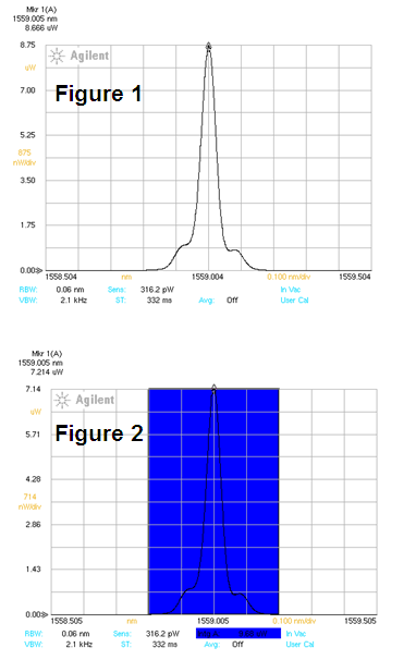
For coherent signals with wide optical spectrum, the traditional scanning method using an OSA or inband polarization method (EXFO) cannot correctly measure system OSNR. Therefore, use the integral method to measure OSNR of coherent signals.

Perform the following operations to measure OSNR using the integral method:

1.Position the central frequency of the wavelength under test in the middle of the screen of an OSA.
2.Select an appropriate bandwidth span for integration (for 40G/100G coherent signals, select 0.4 nm).
3.Read the sum of signal power and noise power within the specified bandwidth. On the OSA, enable the Trace Integ function and read the integral value. As shown in Figure 2, the integral optical      power (P + N) is 9.68 uW.
4.Read the integral noise power within the specified bandwidth. Disable the related laser before testing the integral noise power. Obtain the integral noise power N within the signal bandwidth      specified in step 2. The integral noise power (N) is 29.58 nW.
5.Calculate the integral noise power (n) within the reference noise bandwidth. Generally, the reference noise bandwidth is 0.1 nm. Read the integral power of central frequency within the bandwidth of 0.1 nm. In this example, the integral noise power within the reference noise bandwidth is 7.395 nW.
6.Calculate OSNR. OSNR = 10 x lg{[(P + N) – N]/n}

In this example, OSNR = 10 x log[(9.68 – 0.02958)/0.007395] = 31.156 dB

osnr


We follow integral method because Direct OSNR Scanning Cannot Ensure Accuracy because of the following reason:

A 40G/100G signal has a larger spectral width than a 10G signal. As a result, the signal spectrums of adjacent channels overlap each other. This brings difficulties in testing the OSNR using the traditional OSA method, which is implemented based on the interpolation of inter-channel noise that is equivalent to in-band noise. Inter-channel noise power contains not only the ASE noise power but also the signal crosstalk power. Therefore, the OSNR obtained using the traditional OSA method is less than the actual OSNR. The figure below shows the signal spectrums in hybrid transmission of 40G and 10G signals with 50 GHz channel spacing. As shown in the figure, a severe spectrum overlap has occurred and the tested ASE power is greater than it should be .As ROADM and OEQ technologies become mature and are widely used, the use of filter devices will impair the noise spectrum. As shown in the following figure, the noise power between channels decreases remarkably after signals traverse a filter. As a result, the OSNR obtained using the traditional OSA method is greater than the actual OSNR..


Why does FEC introduce latency?

The addition of FEC overhead at the transmit end and FEC decoding at the receive end cause latency in signal transmission.

Relationship between latency and FEC scheme types

  • To improve the correction capability, more powerful and complex FEC codes must be used. However, the more complex the FEC codes are, the more time FEC decoding will take. As a result, the latency is increased.
  • For a non-coherent 40G signal, AFEC typically introduces a larger latency (60~120 us) than FEC, which introduces a latency of 30 us.
  • Latency of a non-coherent 40G signal is related to the ODUk mapping mode.
  • Latency is also related to the amount of overhead. More overhead means that FEC decoding will take more time.
  • Latency introduced by 100G SD-FEC with 20% overhead > Latency introduced by 100G HD-FEC with 7% overhead
  • In addition, the latency is subject to the signal coding rate. With the overhead unchanged, there will be less latency as the signal rate increases.
  • Latency introduced by 100G HD-FEC < Latency introduced by 40G AFEC

Latency specifications of OTN equipment

Data and storage services are sensitive to latency while OTN services are not. Currently, no international standards have defined how much latency that OTN signals must satisfy. Vendor equipment supports latency testing for different service rates, FEC schemes, and mapping modes. You can recommend a latency value for customers, but latency should not be an acceptance test item. You cannot make a commitment to a latency specification.

Why does coherent detection introduce pre-FEC bit errors?

  • The DSP algorithm at the receive end detects and analyzes the phase and amplitude of a received signal in real time to calculate and compensate the distortion of the signal caused by factors such as CD, PMD, and nonlinearity. Because CD, PMD, and nonlinearity vary with time, the compensation amount calculated by the DSP algorithm is not so accurate and thus pre-FEC bit errors occur.
  • In practice, the transmission distance should be extended as long as possible. The nonlinearity in a long-haul system cause large changes in signal phases. The DSP algorithm is thus required to lock the phase of each signal at a large tracking step, which enables fast locking of great phase changes but has poorer compensation accuracy. As a result, background noise is introduced and further bit errors occur (error floor poorer than 1.0E-6). The background noise is the major factor that causes pre-FEC bit errors in back-to-back OSNR measurement and short-reach transmission. It is negligible compared with the noise introduced in long-haul transmission. Therefore, the large-step tracking method remarkably improves long-haul transmission performance without affecting short-reach transmission performance.
  •  The DSP algorithm is independent of optical-layer configurations, such as back-to-back configurations, the transmission distance, and the number of spans. Therefore, in a back-to-back configuration, the DSP algorithm also has a compensation error and introduces bit errors.

Important Notes on BER for Coherent

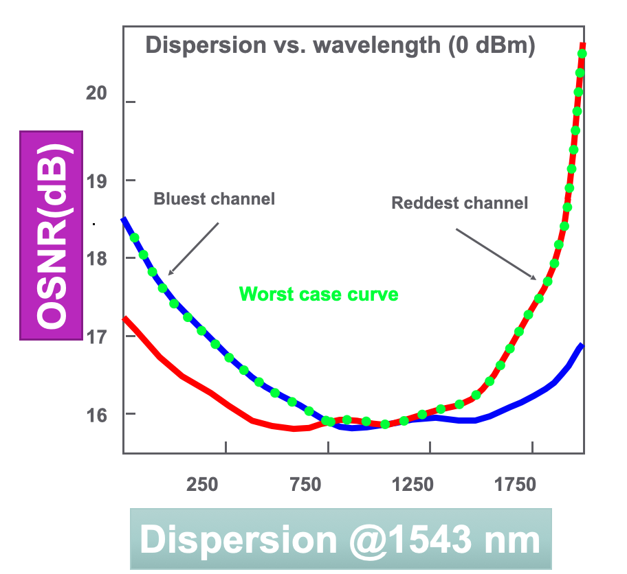
  • For 100G coherent optical modules, the pre-FEC BERs may differ when different 100G boards are connected in back-to-back manner or when WDM-side external loopbacks are performed because of differences in the optical modules. Similarly, after signals traverse spans with good OSNRs, the BERs of different 100G boards may also differ. However, the use of advanced DSP algorithm in the 100G boards ensure that all the 100G boards have the same FEC correction capability.
  • As shown in the figure below, the red and blue lines represent the test data of two different 100G boards.

Basic understanding on Tap ratio for Splitter/Coupler

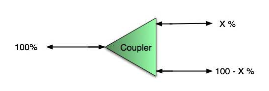
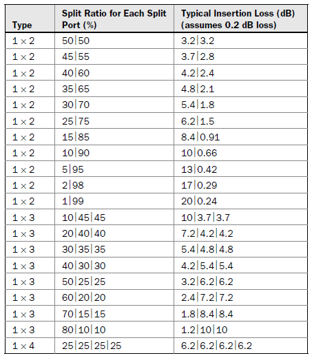
Fiber splitters/couplers divide optical power from one common port to two or more split ports and combine all optical power from the split ports to one common port (1 × coupler). They operate across the entire band or bands such as C, L, or O bands. The three port 1 × 2 tap is a splitter commonly used to access a small amount of signal power in a live fiber span for measurement or OSA analysis. Splitters are referred to by their splitting ratio, which is the power output of an individual split port divided by the total power output of all split ports. Popular splitting ratios are shown in Table below; however, others are available. Equation below can be used to estimate the splitter insertion loss for a typical split port. Excess splitter loss adds to the port’s power division loss and is lost signal power due to the splitter properties. It typically varies between 0.1 to 2 dB, refer to manufacturer’s specifications for accurate values. It should be noted that splitter function is symmetrical.tap ratio

where IL = splitter insertion loss for the split port, dB

Pi = optical output power for single split port, mW

PT = total optical power output for all split ports, mW

SR = splitting ratio for the split port, %

Γe = splitter excess loss (typical range 0.1 to 2 dB), dB

Common splitter applications include

• Permanent installation in a fiber link as a tap with 2%|98% splitting ratio. This provides for access to live fiber signal power and OSA spectrum measurement without affecting fiber traffic. Commonly installed in DWDM amplifier systems.

• Video and CATV networks to distribute signals.

• Passive optical networks (PON).

• Fiber protection systems.

Example with calculation:

If a 0 dBm signal is launched into the common port of a 25% |75% splitter, then the two split ports, output power will be −6.2 and −1.5 dBm. However, if a 0 dBm signal is launched into the 25% split port, then the common port output power will be −6.2 dBm.

Calculation.

Launch power=0 dBm =1mW


Tap is  25%|75%

so equivalent mW power which is linear  will be

0.250mW|0.750mW

and after converting them ,dBm value will be

-6.02dBm| -1.24dBm

Some of the common split ratios and their equivalent Optical Power is available below for reference.tap

Why it is Good to have ORL >30dB for general fiber links?

Optical return loss (ORL) is the logarithmic ratio of the launch (incident) power divided by the total reflected power seen at the launch point. The total reflected power is the total accumulated reflected optical power measured at the launch caused by fiber Rayleigh scattering and Fresnel reflections. Rayleigh scattering is the scattering of light along the entire length of the fiber, caused by elastic collisions between the light wave and fiber molecules. This results in some of the light to be reflected back to the source. Rayleigh scattering is intrinsic to the fiber and therefore cannot be eliminated.

Fresnel reflections occur in the light path where there is an abrupt change in the refractive index such as at connections and splices. The further away a reflective event is from the fiber launch point the less

it contributes to the total reflected power. Therefore, fiber connections and splices closest to the laser contribute the most to the ORL. ORL is always expressed as a positive decibel. The higher the ORL the lower the reflected power.


where ORL = optical return loss, dB

P= total reflected power seen at the launch point, mW

P= launch or incident power, mW


where = backscattering capture coefficient, approximately 0.0015

for standard fiber at 1550 nm

L= fiber length, km

α= attenuation coefficient, 1/km


See calculation for ORL for SMF at 1550nm.

Assume fiber attenuation is 0.22 dB/km at 1550 nm,

= 0.0015 with a nonreflective end.

L=20Km

After calculation using above generic values; ORL will come as ~30 dB.

ITU-T G.959.1 recommends a minimum ORL of 24 dB for 2.5, 10, and 40 Gbps fiber links.

Q is the quality of a communication signal and is related to BER. A lower BER gives a higher Q and thus a higher Q gives better performance. Q is primarily used for translating relatively large BER differences into manageable values.

Pre-FEC signal fail and Pre-FEC signal degrade thresholds are provisionable in units of dBQ so that the user does not need to worry about FEC scheme when determining what value to set the thresholds to as the software will automatically convert the dBQ values to FEC corrections per time interval based on FEC scheme and data rate.

The Q-Factor, is in fact a metric to identify the attenuation in the receiving signal and determine a potential LOS and it is an estimate of the Optical-Signal-to-Noise-Ratio (OSNR) at the optical receiver.   As attenuation in the receiving signal increases, the dBQ value drops and vice-versa.  Hence a drop in the dBQ value can mean that there is an increase in the Pre FEC BER, and a possible LOS could occur if the problem is not corrected in time.

The Quality of an Optical Rx signal can be measured by determining the number of “bad” bits in a block of received data.  The bad bits in each block of received data are removed and replaced with “good” zero’s or one’s such that the network path data can still be properly switched and passed on to its destination.  This strategy is referred to as Forward Error Correction (FEC) and prevents a complete loss of traffic due to small un-important data-loss that can be re-sent again later on.  The process by which the “bad” bits are replaced with the “good” bits in an Rx data block is known as Mapping.  The Pre FEC are the FEC Counts of “bad” bits before the Mapper and the FEC Counts (or Post FEC Counts) are those after the Mapper.

The number of Pre FEC Counts for a given period of time can represent the status of the Optical Rx network signal; An increase in the Pre FEC count means that there is an increase in the number of “bad” bits that need to be replaced by the Mapper.  Hence a change in rate of the Pre FEC Count (Bit Erro Rate – BER) can identify a potential problem upstream in the network.  At some point the Pre FEC Count will be too high as there will be too many “bad” bits in the incoming data block for the Mapper to replace … this will then mean a Loss of Signal (LOS).

As the normal number of Pre FEC Counts are high (i.e. 1.35E-3 to 6.11E-16) and constantly fluctuate, it can be difficult for an network operator to determine whether there is a potential problem in the network.  Hence a dBQ value, known as the Q-Factor, is used as a measure of the Quality of the receiving optical signal.  It should be consistent with the Pre FEC Count Bit Error Rate (BER).

The standards define the Q-Factor as Q = 10log[(X1 – X0)/(N1 – N0)] where Xj and Nj are the mean and standard deviation of the received mark-bit (j=1) and space-bit (j=0)  …………….  In some cases Q = 20log[(X1 – X0)/(N1 – N0)]

For example, the linear Q range 3 to 8 covers the BER range of 1.35E-3 to 6.11E-16.

Nortel defines dBQ as 10xlog10(Q/Qref) where Qref is the pre-FEC raw optical Q, which gives a BER of 1E-15 post-FEC assuming a particular error distribution. Some organizations define dBQ as 20xlog10(Q/Qref), so care must be taken when comparing dBQ values from different sources.

The dBQ figure represents the dBQ of margin from the following pre-FEC BERs (which are equivalent to a post-FEC BER of 1E-15). The equivalent linear Q value for these BERs are  Qref in the above formula.

Pre-FEC signal degrade can be used the same way a car has an “oil light” in that it states that there is still margin left but you are closer to the fail point than expected so action should be taken.

Bit error rate, BER is a key parameter that is used in assessing systems that transmit digital data from one location to another.

BER can be affected by a number of factors. By manipulating the variables that can be controlled it is possible to optimise a system to provide the performance levels that are required. This is normally undertaken in the design stages of a data transmission system so that the performance parameters can be adjusted at the initial design concept stages.

  • Interference:   The interference levels present in a system are generally set by external factors and cannot be changed by the system design. However it is possible to set the bandwidth of the system. By reducing the bandwidth the level of interference can be reduced. However reducing the bandwidth limits the data throughput that can be achieved.
  • Increase transmitter power:   It is also possible to increase the power level of the system so that the power per bit is increased. This has to be balanced against factors including the interference levels to other users and the impact of increasing the power output on the size of the power amplifier and overall power consumption and battery life, etc.
  • Lower order modulation:   Lower order modulation schemes can be used, but this is at the expense of data throughput.
  • Reduce bandwidth:   Another approach that can be adopted to reduce the bit error rate is to reduce the bandwidth. Lower levels of noise will be received and therefore the signal to noise ratio will improve. Again this results in a reduction of the data throughput attainable.

It is necessary to balance all the available factors to achieve a satisfactory bit error rate. Normally it is not possible to achieve all the requirements and some trade-offs are required. However, even with a bit error rate below what is ideally required, further trade-offs can be made in terms of the levels of error correction that are introduced into the data being transmitted. Although more redundant data has to be sent with higher levels of error correction, this can help mask the effects of any bit errors that occur, thereby improving the overall bit error rate.

raman
#raman

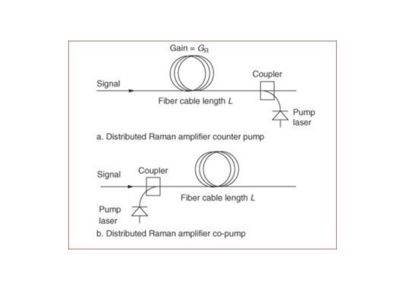
A Raman amplifier is a well-known amplifier configura­tion. This amplifier uses conventional fiber (rather doped fibers), which may be co-or counter-pumped to provide amplification over a wavelength range which is a function of the pump wavelength. The Raman amplifier relies upon forward or backward stimulated Raman scattering. Typically, the pump source is selected to have a wavelength of around 100 nm below the wavelength over which ampli­fication is required.

Keynotes of using Raman Amplifiers:

  • Its usage improves the overall gain characteristics of high capacity optical wavelength division multiplexed (WDM) communications systems.
  • Its usage do not attenuate signals outside the wavelength range over which amplification takes place.
  • it is usual to provide a separate pump sources for each wavelength required  in form of Raman fibre lasers or semiconductor pumps.
  • Multiple lasers increases the overall costs of Raman amplifiers.
  • Raman Amplifiers are very sensitive to input power so they are always used with EDFA in cascaded fashion.( a small change at input will result in high output power change and thus subsequent components may suffer)
  • Power consumption  is very high as multiple lasers are used.
  • Always keep output shut-off while integrating Raman in a link as high power lasers are dangerous to personnel too.
  • Raman ampliers are typically pumped using unpolarized pump beams.i.e (both the pump and the signal propagate in the fundamental mode, supports two orthogonal polarization states in each mode. Thus, even though the fiber is single mode, the pump and signal may propagate in orthogonal polarizations.)

Distributed (Raman) Gain Improved Transmission Systems


Figure 1 shows a conventional transmission system using erbium-doped fiber amplifiers (EDFAs) to amplify the signal. The signal power in the transmission line is shown; at the output of the EDFA the signal power is high. However, nonlinear effects limit the amount of amplification of the signal. The signal is attenuated along the transmission line. In addition, the minimum signal level limits the Optical Signal to Noise Ratio (OSNR) of the transmission. So the transmission distance between each amplifier point is limited by nonlinear effects at the high signal level right after amplification and the minimum allowable OSNR just before amplification.

Figure 2. Amplification scheme using distributed Raman amplification together with lumped EDFAs

By comparison, Figure 2 shows a scenario where distributed Raman amplification is used. In this hybrid version with backward propagating pumps and EDFAs, the signal power level evolves as shown by the red curves. At the end of the link, the signal is amplified by the Raman pump, and the OSNR is thereby improved. The input power level can also be lowered, as Raman amplification keeps the signal from the noise limit. The lower input power mitigates the non-linearities in the system. Forward propagating pumps or a combination of both forward and backward propagating pumps may be used. Installing transmission fibers that have been designed and optimized to take full advantage of the Raman technology allows system designs with higher capacity and lower cost.

Characteristics of Raman-Optimized Fibers

Fibers optimized for Raman amplification offer the following characteristics:

  • high Raman gain efficiency
  • low attenuation at signal and pump wavelengths
  • low zero dispersion wavelength.

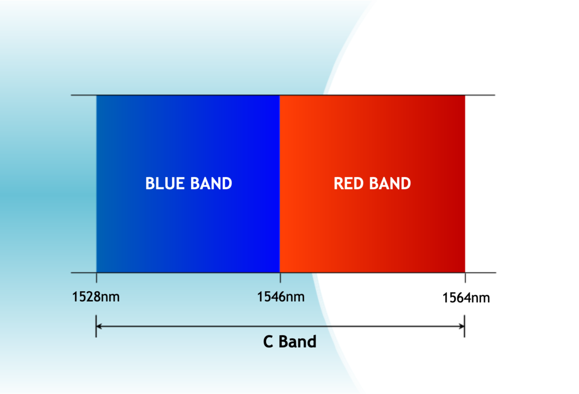
The ITU approved DWDM band extends from 1528.77 nm to 1563.86 nm, and divides into the red band and the blue band.

red blue

The red band encompasses the longer wavelengths of 1546.12 nm and higher.

The blue band wavelengths fall below 1546.12 nm.

This division has a practical value because useful gain region of the lowest cast EDFAs corresponds to the red band wavelengths. Thus, if a system only requires a limited number of DWDM wavelengths using the red band wavelength yields the lowest overall system cost.

Regarding Red and Blue convention.

Its just a convention which is prevalent since electromagnetic spectrum is in study either it is Doppler effect or Rayleigh Scattering and later on it was taken into consideration in optics or photonics world.

(Taken from Wikipedia: Its more of talking light spectrum VIBGYOR where red-shift and blue-shift is discussed and  “red-shift “ happens when light or other electromagnetic radiation from an object is increased in wavelength, or shifted to the red end of the spectrum.In general, whether or not the radiation is within the visible spectrum, “redder” means an increase in wavelength – equivalent to a lower frequency and a lower photon energy,A blueshift is any decrease in wavelength, with a corresponding increase in frequency, of an electromagnetic wave; the opposite effect is referred to as redshift. In visible light, this shifts the colour from the red end of the spectrum to the blue end.)

The ITU approved DWDM C-band extends from 1528.77 nm to 1563.86 nm, and divides into the red band and the blue band.

The red band encompasses the longer wavelengths of 1546.12 nm and higher.

The blue band wavelengths fall below 1546.12 nm.

Example to make it more clear:-

C Band: 1528.77 nm to 1563.86 nm

C-Blue 1529.44~1543.84

=====guardband====

C-red 1547.60~1561.53


L Band: 1565nm-1625nm

L-Blue: 1570nm-1584nm

=====guardband====

L-Red: 1589nm-1603nm

So, this blue and red shift is for characterisation behaviour study and to classify filters as well .

As defined in G.709 an ODUk container consist of an OPUk (Optical Payload Unit) plus a specific ODUk Overhead (OH).    OPUk OH information is added to the OPUk information payload to create anOPUk.  It includes information to support the adaptation of client signals.Within the OPUk overhead there is the payload structure identifier (PSI) that includes the     payload type (PT).  The payload type (PT) is used to indicate the composition of the OPUk signal.

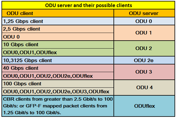
When an ODUj signal is multiplexed into an ODUk, the ODUj signal is first extended with frame alignment overhead and   then mapped into an Optical channel Data Tributary Unit (ODTU). Two different types of ODTU are   defined in G.709:

– ODTUjk ((j,k) = {(0,1), (1,2), (1,3), (2,3)}; ODTU01,ODTU12,ODTU13 and ODTU23) in which an ODUj signal is mapped via the asynchronous mapping procedure (AMP), defined in clause 19.5 of G.709.

– ODTUk.ts ((k,ts) = (2,1..8), (3,1..32), (4,1..80)) in which a lower order ODU (ODU0, ODU1, ODU2, ODU2e, ODU3, ODUflex) signal is mapped via the generic mapping procedure (GMP), defined in clause 19.6 of  G.709.

When PT is assuming value 20 or 21,together with OPUk type (K=1,2,3,4), it is used to discriminate two different  ODU multiplex structure ODTUGx :

 Value 20: supporting ODTUjk only,

– Value 21: supporting ODTUk.ts or ODTUk.ts and ODTUjk.

The discrimination is needed for OPUk with K =2 or 3, since OPU2 and OPU3 are able to support both the different ODU multiplex structures.For OPU4 and OPU1, only one type  of ODTUG is supported: ODTUG4 with PT=21 and ODTUG1 with PT=20.The relationship between PT and TS granularity, is in the fact that the twodifferent ODTUGk discriminated by PT and OPUk  are characterized by two different TS granularities of the relatedOPUk, the former at 2.5   Gbps, the latter at 1.25Gbps.

To detect a failure that occurs at the source (e.g., laser failure) or the transmission facility (e.g., fiber cut), all incoming SONET signals are monitored for loss of physical-layer signal (optical or electrical). The detection of an LOS defect must take place within a reasonably short period of time for timely restoration of the transported payloads.

A SONET NE shall monitor all incoming SONET signals (before descrambling) for an “all-zeros patterns,” where an all-zeros pattern corresponds to no light pulses for OC-N optical interfaces and no voltage transitions for STS-1 and STS-3 electrical interfaces. An LOS defect shall be detected when an all-zeros pattern on the incoming SONET signal lasts 100 μs or longer. If an all-zeros pattern lasts 2.3 μs or less, an LOS defect shall not be detected. The treatment of all-zeros patterns lasting between 2.3 μs and 100 μs for the purpose of LOS defect detection is not specified and is therefore left to the choice of the equipment designer. For testing conformance to the LOS detection requirement, it is sufficient to apply an all-zeros pattern lasting at most 2.3 μs, and to apply an all-zeros pattern lasting at least 100 μs.

Note that although an all-zeros pattern that lasts for less than 2.3 μs must not cause the detection of an LOS defect, an NE that receives a relatively long (in terms of the number of bit periods) all-zeros pattern of less than 2.3 μs is not necessarily expected to continue to operate error-free through that pattern.For example, in such cases it is possible that the NE’s clock recovery circuitry may drift off frequency due to the lack of incoming pulses, and therefore the NE may be “looking in the wrong bit positions” for the SONET framing pattern after the all-zeros pattern ends. If this occurs, it will continue for approximately 500 μs, at which point the NE will detect an SEF defect. The NE would then perform the actions associated with SEF defect detection (e.g., initiate a search for the “new” framing pattern position),rather than the actions associated with LOS defect detection (e.g., AIS and RDI insertion, possible protection switch initiation). In addition to monitoring for all-zeros patterns a SONET NE may also detect an LOS defect if the received signal level (e.g., the incoming optical power) drops below an implementation-determined threshold.