
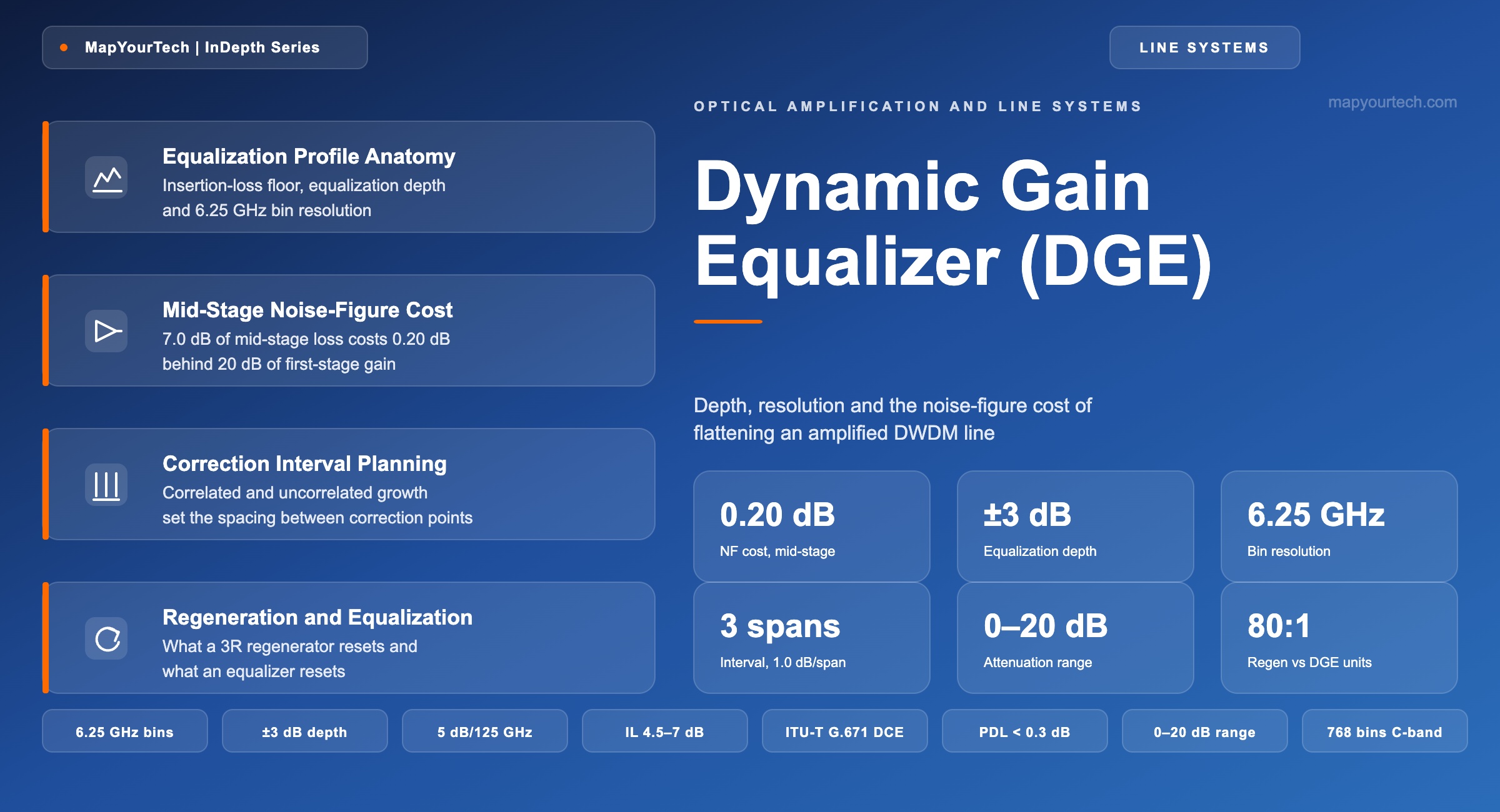
Dynamic Gain Equalizer (DGE) in Optical Line Systems
The device that draws the inverse of an amplified line's spectral shape: how equalization depth and bin resolution are specified, what mid-stage placement costs in noise figure, and how far apart correction points can sit.
An amplifier is flat across the band it was calibrated for.
What You Will Learn
- Define the equalization profile from its three parts in Section 2 and read Figure 1: a 4.50 dB insertion-loss floor, a 2.40 dB equalization depth, and an output flat at −6.36 dB.
- Separate the four sources of spectral shape in Section 3 by signature, and tell a 0.83 dB/THz Raman tilt apart from a 1.0 dB per-span ripple structure fixed to wavelength.
- Place the device inside a two-stage amplifier using Figure 3, and price 7.0 dB of mid-stage loss at 0.20 dB of noise figure against 7.00 dB at the input.
- Convert a bin grid into a resolution limit: 6.25 GHz bins give 768 addressable points across 4.8 THz, and a 40 dB/THz slope limit bounds how sharp a commanded feature can be.
- Set the equalization interval from Section 6 and Table 2: three spans at 1.0 dB of Raman ripple per span, eight spans at 0.35 dB, for the same 3.0 dB flatness budget.
- Read the two accumulation laws in Figure 6: 12.0 dB after twelve unequalized spans against 1.04 dB when each span is corrected to a 0.30 dB residual.
- Run the commissioning loop of Figure 4 to its exit criteria, and set the loop gain of Section 5.4 to 0.3–0.5 so the profile converges over several cycles instead of oscillating around the target.
- Select a correction technology from Table 6, separate what a 3R regenerator resets from what an equalizer resets in Table 7, and price the difference at 8 modules against 640 line modules on the same 12-amplifier line at 80 carriers.
1. Introduction
A dynamic gain equalizer (DGE) is a wavelength-dependent optical attenuator whose loss-versus-frequency profile can be commanded while traffic runs. It occupies the mid-stage of a line amplifier or sits as a separate module beside it, and it subtracts the spectral shape that the preceding span and amplifier added. Everything else in an amplified line either adds a shape or scales one: the erbium medium adds its gain curve, the fibre adds a loss slope and a Raman transfer, a variable optical attenuator (VOA) scales the whole band by one number. The equalizer is the only element on the line that can apply a different loss at 191.4 THz than at 196.0 THz and change that difference by software an hour later.
The device class has a standards name that differs from the one the industry uses. ITU-T G.671, which specifies transmission characteristics of optical components and subsystems, covers it as a dynamic channel equalizer (DCE) and lists attenuation range among the parameters specifiable for it. Vendor documentation and field practice say dynamic gain equalizer, and that is the term used here; the two name the same function, and a specification written against one is read against the other.
The reason the device exists is arithmetic rather than aesthetics. Identical amplifiers built to one design carry identical residual gain shape, and identical errors add linearly down a cascade instead of averaging out. A 0.35 dB per-span residual that nobody would measure on a single amplifier reaches 4.2 dB after twelve spans, and 4.2 dB of spread means the worst channel has surrendered the entire optical signal-to-noise ratio (OSNR) difference between dual-polarization 16-state quadrature amplitude modulation (DP-16QAM) and dual-polarization quadrature phase-shift keying (DP-QPSK). Raman-assisted lines make the arithmetic worse: deployed characterisation of counter-propagating Raman amplification puts gain ripple at about 1.0 dB per span, so a line that would have needed one correction point every eight spans now needs one every three.
Deployment has followed that arithmetic into the line card. In-line amplifiers from current optical line systems carry the equalizer as an embedded function alongside an optical channel monitor (OCM), rather than as an optional chassis module: one vendor documents embedded continuous dynamic gain equalization on its in-line amplifier line cards, stated purpose being to compensate gain ripple caused by Raman amplification or to apply pre-emphasis for C+L-band line systems. Component suppliers have pushed in the same direction: Lumentum demonstrated a multi-rail equalizer combining eight equalizers with 16 channel monitors for two fibre pairs carrying C-band and L-band traffic at OFC in March 2026, on the company's own figures.
This article treats the equalizer as a device with a specification sheet and a control loop, not as a network-level flatness policy. Section 2 defines the attenuation profile and its parts. Section 3 names the shapes it has to cancel. Sections 4 and 5 give the architecture and the arithmetic that governs depth, resolution and noise figure. Sections 6 through 9 cover placement, commissioning, monitoring and fault diagnosis. Sections 10 through 13 compare the alternatives, look at multi-band operation, and close with a reference sheet. The network-level view of where flatness belongs in a line system is treated separately in the MapYourTech analysis of spectral power management at scale.
Takeaway: An equalizer buys flatness with insertion loss. The design question is never whether the device helps but whether the loss it inserts, placed where it is placed, costs less OSNR than the spread it removes.
2. Equalization Profile Definition and Component Terms
An equalization profile is the loss-versus-frequency function a dynamic gain equalizer applies to a wavelength-division-multiplexed signal, expressed in decibels and sampled on a fixed frequency grid. It has two parts: a fixed insertion-loss floor present at every frequency, and a commandable excess loss that is zero at the most transparent frequency and positive everywhere else. The peak-to-peak range of that excess loss is the equalization depth.
2.1 Distinctions From the Adjacent Quantities
Four pairs of terms get conflated in practice, and each confusion produces a different specification error.
Insertion loss against equalization depth. Insertion loss is the floor the device adds even when it is commanded flat; equalization depth is how far above that floor the deepest bin can go. A device quoted at "6.9 dB loss" with a 2.40 dB depth adds 4.50 dB at its most transparent bin, and the amplifier has to supply that 4.50 dB whether any equalization is commanded or not.
Read the Full Analysis with Premium
The remaining 89% of this article — the design numbers, trade-offs and field guidance — is part of MapYourTech Premium, along with the full premium library, courses and professional tools.
You May Also Like
-
Free
-
September 4, 2026
-
Premium
-
September 4, 2026
-
Premium
-
September 4, 2026