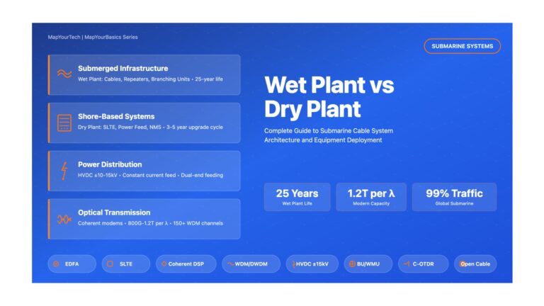
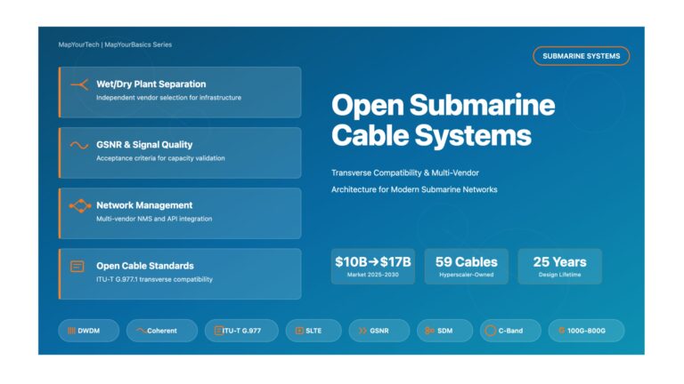
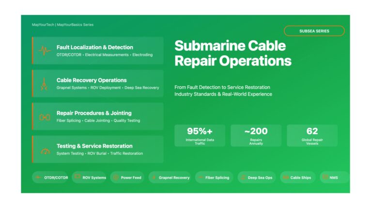
Submarine Cable Repair Operations – Comprehensive Visual Guide Overview of Submarine Cable Repair Operations Technical Guide Based on Industry Standards...
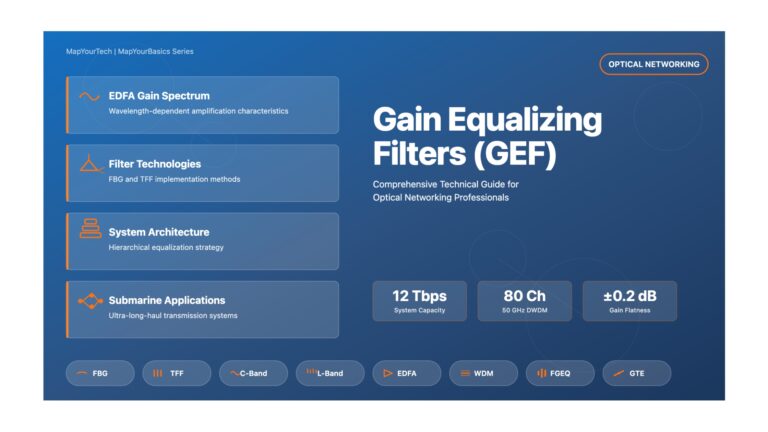
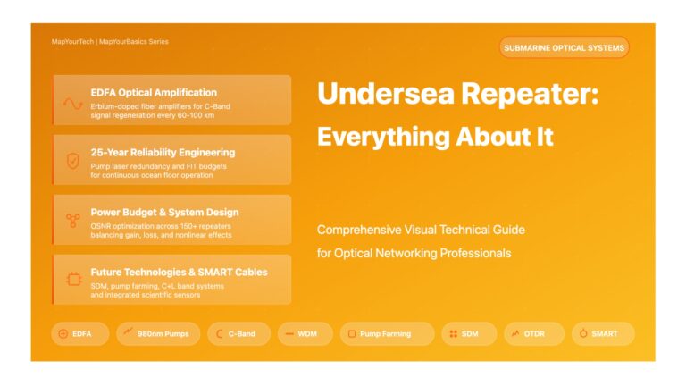
Undersea Repeater: Everything About It – Comprehensive Visual Guide Undersea Repeater: Everything About It Comprehensive Visual Technical Guide for Optical...