Optical Circuit Switching: MEMS Steering and Loss Budgets
Mirror steering sets the port count, transparency sets the service life, and insertion loss decides whether the switch fits the link at all.
The best network design is one that anticipates tomorrow's needs.
1. Introduction
An optical circuit switch (OCS) connects one input fiber to one output fiber by tilting a pair of micro-mirrors into alignment. There is no optical-electrical-optical (OEO) conversion, no packet header is read, and nothing is buffered. The device behaves as a steerable patch panel that reconfigures under software control in milliseconds, and the light that leaves an output port is the same light that entered the input port, delayed by propagation and reduced by loss.
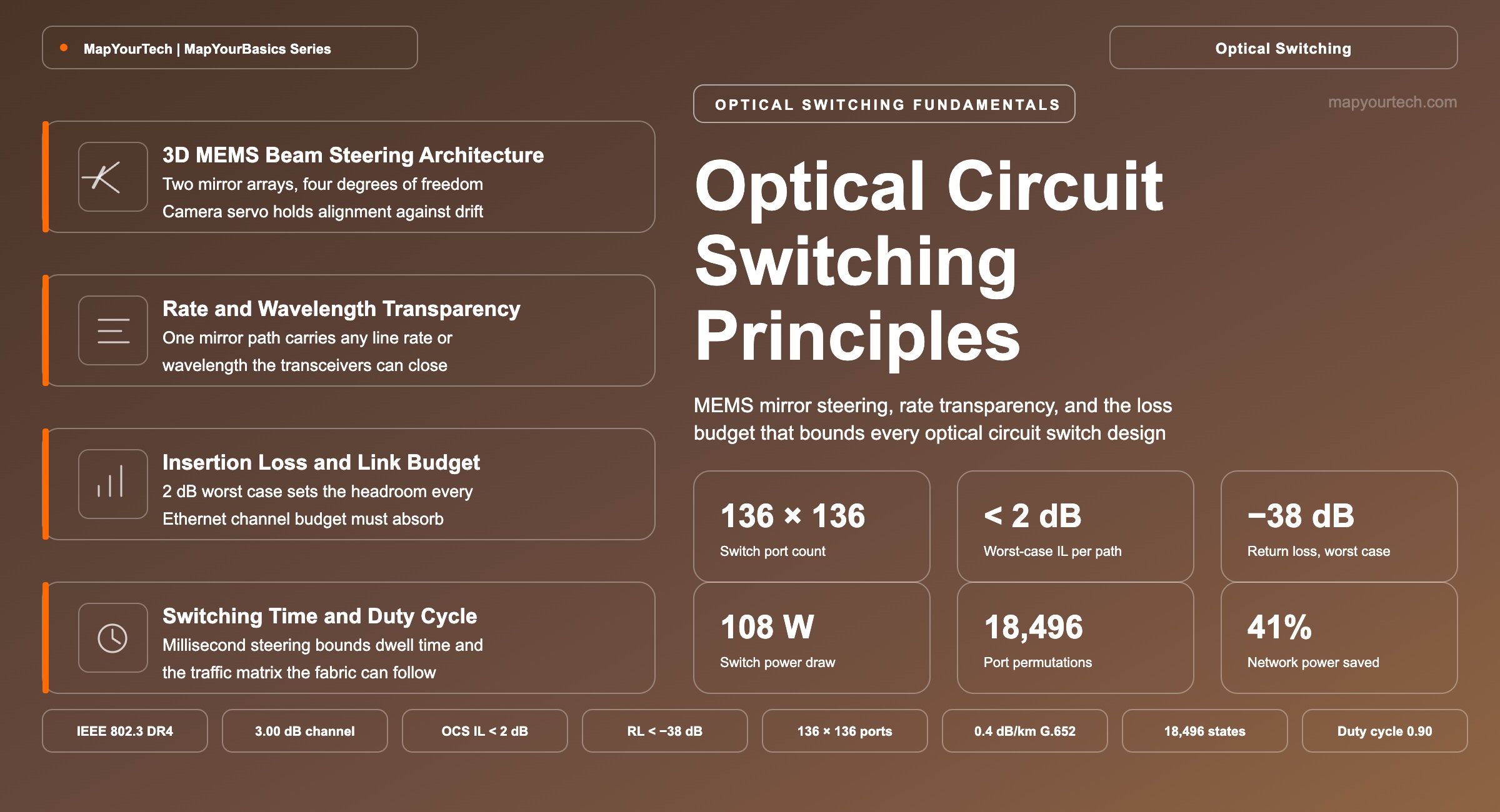
Google's Apollo layer, described in an ACM SIGCOMM paper as the first large-scale production deployment of optical circuit switching for data center networking, put tens of thousands of 136 × 136-port switches into service. Each draws a maximum of 108 W, a fraction of an electrical packet switch (EPS) of the same switching capacity (operator-reported). Replacing the aggregation spine with an OCS layer and moving to a direct-connect topology produced a 41% reduction in network power and a 30% reduction in capital cost across the Jupiter fabric (measured results, ACM SIGCOMM), which moved the technology out of research testbeds and into production data center and interconnect architecture.
Three quantities decide whether an OCS fits a network. The beam-steering mechanism sets port count and switching time. Transparency of the optical path sets how many transceiver generations the hardware survives. Insertion loss decides whether the surrounding link budget can absorb the device at all, and it is what most often rules an OCS out. This article covers each in turn and works the loss allocation through on a 400GBASE-DR4 channel.
2. Three-Dimensional MEMS Beam Steering Architecture
Three-dimensional MEMS beam steering places two mirror arrays in series, and the reason for two rather than one is geometric. A single tilting mirror can aim a beam at any output port, but the beam arrives at an angle the receiving collimator will not accept and most of the power is lost at the coupling. The second mirror corrects that angle and delivers the beam along the collimator's optical axis. Each mirror tilts about two orthogonal axes, so one connection is defined by four controlled angles.
Light enters through a two-dimensional fiber collimator array: an N × N fiber array bonded to a lens array that turns each fiber output into a collimated free-space beam. The beam from input port i strikes mirror i in the first array, is deflected onto mirror j in the second, and is redirected into output collimator j. Every input owns a mirror in the first array and every output owns one in the second, so the fabric is strictly non-blocking: any input reaches any output without disturbing an existing connection.
Actuation is electrostatic. Comb-drive structures rotate each gold-coated mirror, and the drive voltages run from one to a few hundred volts. The mirrors present a capacitive load, so holding a position costs almost nothing once set: a well-designed high-voltage driver consumes on the order of tens of milliwatts per mirror and port, which is what lets a whole 136 × 136 system fit inside 108 W (operator-reported).
Alignment is closed-loop. Each MEMS array is illuminated with 850 nm monitor light, and the reflected monitor beams are imaged by a camera module; a servo reads the image and adjusts the mirror drive to minimise loss on the signal path. Using one camera image per array, instead of a photodetector per mirror, is the choice that made the switch manufacturable in volume — it removes N monitoring channels from the bill of materials and from the assembly process at once.
Yield sets the usable radix. Each die in the Apollo switch carries 176 individually controllable mirrors, of which 136 are selected during calibration. Every one of the resulting 136 × 136 = 18,496 connection states has its own stored pair of drive voltages, measured at the factory and held in the unit. The switch does not compute a mirror angle at run time; it recalls a measured one.
Takeaway: port count in a three-dimensional MEMS switch is bounded by mirror yield and by the angular range the two-array geometry covers, not by any electronic throughput limit. The electronics only hold a voltage.
3. Rate and Wavelength Transparency
Every element in the signal path is passive and broadband: two lens arrays, two gold-coated mirrors, and the anti-reflection windows that seal each MEMS package. Nothing in that path is tuned to a symbol rate, a modulation format, a framing structure, a line code, or a forward error correction (FEC) scheme. The switch does not know what it is carrying, and that is the largest architectural difference between an OCS and a packet switch.
The practical result is generational reuse. The Apollo layer carried four generations of optical interconnect — 40, 100, 200 and 400 GbE — through the same hardware on the same CWDM4 wavelength grid, with backward compatibility engineered into the transceivers rather than the switch. Switch capital cost then amortises over the lifetime of the building, like power and cooling plant, rather than over the life of a pluggable transceiver generation.
Transparency has boundaries, and three bind in practice. The first is optical coating: the package window and the lens coatings must pass both the data wavelengths and the 850 nm monitor wavelength with low loss, and in a two-array design each data path makes eight passes through window coatings. Widening the passband to cover the O, S, C and L bands at once holds return loss to a tighter tolerance across a much wider spectrum. The second is fiber type, since three-dimensional MEMS steering is a single-mode technique. The third is reflection sensitivity, which rises with PAM order and is covered in Section 5.
Wavelength-selective switching is often grouped with this, and the contrast is worth drawing. A switch built on an arrayed waveguide grating (AWG) fixes channel spacing and width in hardware, so the wavelength plan and the achievable line rate are set at purchase. A liquid crystal on silicon (LCoS) wavelength selective switch (WSS) — the component at the heart of a modern reconfigurable optical add-drop multiplexer — is wavelength-selective by construction, and its filter shape carries a spectral cost: cascaded passbands narrow with each traversal and drive the guard band allocation for the line system. A MEMS OCS port has no filter shape and no channel plan: it carries whatever wavelength comb arrives on the fiber.
Rate transparency is an architectural property, not a specification line. It moves the switching layer out of the networking refresh cycle and into the facility, which changes how the asset is depreciated as much as how it is engineered.
4. Insertion Loss and the Transceiver Link Budget
Insertion loss decides whether an optical circuit switch can be inserted at all. Every decibel the switch consumes comes out of the same channel allowance that has to cover the fiber, the connectors and the transceiver's own margin. Inside the switch, loss accumulates from mirror reflectivity, the eight passes through package window coatings, the two collimator array interfaces, and the splice and connector loss at the front panel.
The Apollo paper reports typical insertion losses below 2 dB across all 18,496 permutations of a 136 × 136 switch, with a worst case of 2 dB, and attributes the tail of the distribution to splice and connector variation rather than to the mirror path. It names below 2 dB as the design target for data center use, because cost-effective transceivers with moderate power budgets cannot absorb more. Current products specify lower: one MEMS platform at 300 × 300 ports states a typical insertion loss of 1.5 dB or less (vendor claim).
ILOCS,max = ILchannel − α · L − ILconn − ILcirc- Where:
- ILOCS,max — insertion loss the switch may consume, in dB. Typical planning target 1.5–2.0 dB.
- ILchannel — channel insertion loss allowance for the Ethernet physical medium dependent (PMD) sublayer, in dB. Standard-specified in IEEE Std 802.3; 1.8–6.3 dB across the PMDs in Table 1.
- α — fiber attenuation coefficient, in dB/km. ITU-T G.652 specifies a maximum of 0.4 dB/km in the 1310 nm region.
- L — one-way fiber length, in km. Typically 0.1–0.5 km for a home-run inside a data center hall.
- ILconn — total mated-connector and splice loss, in dB. Typically 0.2–0.35 dB per mated angled physical contact (APC) pair.
- ILcirc — circulator loss where bidirectional operation is used, in dB. Typically 0.6–1.0 dB per pair.
Practical Example — loss headroom on a 400GBASE-DR4 channel
IEEE Std 802.3 allows a maximum channel insertion loss of 3.0 dB for 400GBASE-DR4 over 500 m of single-mode fiber (standard-specified). Take a home-run link of 300 m of ITU-T G.652 fiber at 0.4 dB/km, which contributes 0.12 dB, and two mated APC pairs at 0.25 dB each, which contribute 0.50 dB (typical planning values). No circulator is fitted on this link.
ILOCS,max = 3.00 − 0.12 − 0.50 − 0 = 2.38 dB
A switch specified at 2.0 dB worst case fits, with 0.38 dB spare. Run the same fiber plant on a 400GBASE-LR4 channel, where the allowance is 6.3 dB over 10 km (standard-specified), and the headroom rises to 5.68 dB — enough for the switch, a circulator pair and a second patch point.
| PMD | Fiber and reach | Channel loss allowance (dB) | Assumed plant loss (dB) | Available to the switch (dB) |
|---|---|---|---|---|
| 400GBASE-SR4 | OM4 multimode, 100 m | 1.80 | n/a | n/a |
| 400GBASE-DR4 | Single-mode, 500 m | 3.00 | 0.62 | 2.38 |
| 400GBASE-LR4 | Single-mode, 10 km | 6.30 | 0.62 | 5.68 |
| 100GBASE-LR4 | Single-mode, 10 km | 6.30 | 0.62 | 5.68 |
Channel loss allowances in Table 1 are standard-specified in IEEE Std 802.3. Assumed plant loss is the 0.62 dB worked above and applies to the single-mode rows only; the 400GBASE-SR4 entry is marked not applicable because three-dimensional MEMS steering is a single-mode technique.
Takeaway: reserve the switch's loss allocation before selecting the transceiver class. On short single-mode runs the switch, not the fiber, is the dominant loss term, and a DR-class module can fail a 500 m link that an LR-class module closes with margin to spare.
5. Return Loss and Bidirectional Link Impairments
Doubling the effective radix of an optical circuit switch costs nothing in switch hardware and a great deal in reflection discipline. An optical circulator is a three-port non-reciprocal device: light entering port 1 leaves at port 2, and light entering port 2 leaves at port 3. Fitting one at each end converts a duplex transceiver into a bidirectional one, so transmit and receive share a single fiber strand and a single switch port. Apollo uses this to halve both fiber count and port count, and the switch is unchanged because its optical path is reciprocal.
The cost is that counter-propagating signals now occupy the same fiber and the same mirror path. The two beams do not interact with each other, but any reflection along the path — from a connector, a collimator interface, or the circulator — returns power that superposes directly on the received signal. That is multi-path interference (MPI), and it degrades signal-to-noise ratio without changing average received power, so it does not appear on a power meter. Reflectance, not loss, is the measurement that catches it.
Return loss requirements follow from that. The Apollo switch specifies better than −38 dB with a typical measured value of −46 dB, and identifies the interface between the fiber array and the two-dimensional lens array in the collimators as the dominant reflection source (operator-reported). A current 300 × 300 MEMS platform states better than −50 dB (vendor claim). Four measures keep MPI inside the budget:
- APC connectors on every mated pair, and home-run fiber runs with no intermediate patch panels.
- Higher transmitter extinction ratio. The Apollo transceiver line moved from directly modulated lasers (DML) to externally modulated lasers (EML) partly for this reason.
- MPI mitigation implemented in the receiver's digital signal processing (DSP).
- An FEC selected for the higher link budget of the switched path rather than for the nominal PMD budget.
Four-level pulse amplitude modulation (PAM4) sharpens the requirement. For the same optical modulation amplitude, the separation between adjacent PAM4 levels is one third of the on-off keyed equivalent, so identical reflected power consumes three times as much eye margin. Every step up in per-lane rate that arrives through a higher-order format tightens the reflectance specification on a bidirectional switched link.
Takeaway: on a bidirectional link through an OCS, return loss binds as hard as insertion loss and is far less visible. Specify it explicitly, test reflectance rather than loss alone, and keep the mated-pair count low.
6. Switching Time and Control Plane Requirements
Reconfiguration in a three-dimensional MEMS switch is millisecond-scale. Commercial switches typically take 10–20 ms, limited by control software and mirror settling rather than by the mirror mechanics alone, and the Apollo paper describes its own switch in the same terms. That is enough for the operations it serves: topology engineering, fabric expansion and technology refresh are all measured in minutes or longer.
Because the switch is slow relative to a packet, the control plane has to be central. An OCS cannot buffer a packet or read a header, so it cannot make the local forwarding decisions an electrical packet switch makes from a routing table. Connection state arrives instead from a software-defined networking controller that collects demand across the fabric and computes a matching. Throughput of the resulting circuit-switched fabric is set by the duty cycle.
D = Tdwell / (Tdwell + Tswitch)- Where:
- D — fraction of time the fabric carries traffic, dimensionless. Above 0.90 is the working target for a high-throughput fabric.
- Tdwell — time the switch holds one configuration, in ms.
- Tswitch — system-level switching time, in ms. Includes the receiver's lock time, not only the mirror transition; typically 10–20 ms for deployed three-dimensional MEMS hardware.
Put numbers through it. With Tswitch at 15 ms and a target duty cycle of 0.90, the dwell time has to be at least 135 ms. That single result explains why per-flow optical switching stays in the laboratory: it needs burst-mode receivers and microsecond-class fabrics, not the millisecond-class hardware in production today.
Latency behaves differently and favours the OCS everywhere. Added delay through the switch is propagation only: roughly 5 ns per metre in fiber and 3.3 ns per metre in free space. An electrical packet switch of the same capacity adds tens to hundreds of nanoseconds per hop for serialisation and forwarding, so removing a spine tier removes delay as well as power. Individually these are small terms against an end-to-end latency budget, and material once several hops are removed — the same accounting that separates framing and FEC delay in coherent pluggables from fiber propagation.
Takeaway: match the switching timescale to the traffic timescale. Millisecond reconfiguration fits provisioning, topology engineering and scheduled training patterns; it does not fit per-packet forwarding.
7. Optical Switch Technology Comparison
Five switching mechanisms have reached commercial form, and the Apollo paper compares them on the axes a data center cares about: port count, switching time, insertion loss and drive voltage. The trade-off Table 2 exposes is fixed rather than incidental — port count, switching time and insertion loss cannot all be optimised in one architecture, which is why several mechanisms remain in the market.
| Mechanism | Relative cost | Port count | Switching time | Insertion loss (dB) | Drive voltage | Latching |
|---|---|---|---|---|---|---|
| Three-dimensional MEMS | Medium | 320 × 320 | Milliseconds | < 3.0 | Hundreds of volts | No |
| Robotic patch panel | Medium | 1008 × 1008 | Minutes per connection | < 1.0 | Not applicable | Yes |
| Piezoelectric | High | 384 × 384 | Milliseconds | < 2.5 | Tens of volts | No |
| Guided wave | Low | 16 × 16 | Milliseconds | < 6.0 | About 1 volt | No |
| Wavelength switching | Not established | 100 × 100 | Nanoseconds | < 6.0 | Zero | Yes |
Values are as published by the operator at the port count shown, and the insertion loss figures include connector losses. Robotic cross-connects give the lowest loss and highest radix but reconfigure one connection at a time, which suits fiber-plant automation rather than traffic-driven switching. Guided-wave and wavelength-switched fabrics are fast and integrated but lose too much light and scale to too few ports for a spine replacement. Three-dimensional MEMS sits where the data center requirement sits, while piezoelectric actuation holds an advantage in insertion and return loss.
As of 2026 the field has widened from a single operator project into a multi-vendor market. The Open Compute Project formed an Optical Circuit Switching subproject in 2025, co-led by member companies and including hyperscale operators and switch suppliers, to develop open and interoperable OCS specifications; its April 2026 white paper surveys robotic, MEMS, liquid-crystal, piezo-actuated and silicon-photonic approaches side by side. Publicly released market analysis projects OCS revenue above $2.5 billion in 2029 (third-party forecast), and commercial MEMS platforms are shipping at 64 × 64 and 300 × 300 radix.
8. Deployment Practice and Design Constraints
Fiber plant design does most of the work. Home-run fibers with APC connectors mating directly into the switch and circulator chassis keep both insertion and return loss at their minimum, and every patch panel removed from the path removes two mated pairs from the budget. Single-mode fiber throughout is a requirement rather than a preference. Across a data center hall, where reach is short and loss dominates over dispersion, link design is a loss exercise and nothing else.
Availability is engineered at the chassis and at the floor. The Apollo switch operates power supplies in 1+1 and fan modules in 2+2 redundancy, both hot-swappable, and makes the high-voltage driver boards field-replaceable because high-voltage operation is the largest single reliability exposure in a MEMS switch. Spare ports carry the rest: 8 of the 144 available ports are held spare in a 136 × 136 configuration. Latching operation, where the mirror state survives a power event, is desirable but not universal; where the mechanism does not latch, infrastructure power redundancy compensates.
Failure domains are separated physically. Apollo splits a maximum of 256 switches across four zones on the data center floor, feeds each zone from dual power circuits, and reserves a 60 kW uninterruptible power supply per fabric with 30 kW on each feed. Fiber distribution runs in three layers with two drops, and the main distribution trays are physically separated — the same diversity discipline used in transport topology design, applied inside a building.
Reconfiguration follows a fixed sequence worth writing into the runbook: drain the affected links, reconfigure the switch, run a cable audit to confirm baseline packet transmission, run a bit error ratio test, then release to production traffic. Skipping the audit is how a mirror that settled at a marginal angle reaches production as an intermittent fault. Alongside the power and capital savings quoted in Section 1, the same fabric reported a fivefold increase in speed and capacity and threefold faster reconfiguration than the patch-panel interconnect it replaced (measured results, ACM SIGCOMM) — savings of the same character as the power-per-bit case for router-hosted optics.
Takeaway: an OCS deployment is a fiber-plant and availability project more than a switching project. Loss budget, mated-pair count, spare ports, and failure-domain separation decide the outcome; the mirrors are the reliable part.
9. Summary
An optical circuit switch steers light between fiber ports with two arrays of two-axis MEMS mirrors, giving four controlled angles per connection and a strictly non-blocking fabric. Because the path is passive and broadband, the switch is transparent to rate, format and wavelength, and the same hardware has carried four generations of Ethernet interconnect from 40 to 400 GbE. Insertion loss is the binding design constraint: 2 dB worst case in production hardware, against a 3.0 dB standard-specified channel allowance for 400GBASE-DR4 that leaves 2.38 dB after a realistic fiber plant. Return loss is the second constraint and the easier one to miss, because bidirectional operation through circulators turns every reflection into multi-path interference.
Quick reference values for planning: worst-case switch insertion loss 2.0 dB and typical vendor-specified figures near 1.5 dB; return loss better than −38 dB, with −50 dB claimed on current platforms; switching time 10–20 ms; added delay near 3.3 ns per metre of free-space path; 108 W for a 136 × 136 system; and a duty cycle target above 0.90, which sets a minimum dwell time of 135 ms at a 15 ms switching time. For further reading, the Apollo and Jupiter papers carry the deployment data, IEEE Std 802.3 carries the channel allowances, and the Open Compute Project white paper surveys the mechanisms now competing for the same socket.
References
- R. Urata et al., Mission Apollo: Landing Optical Circuit Switching at Datacenter Scale, ACM SIGCOMM.
- L. Poutievski et al., Jupiter Evolving: Transforming Google's Datacenter Network via Optical Circuit Switches and Software-Defined Networking, ACM SIGCOMM.
- IEEE, IEEE Std 802.3 — Standard for Ethernet, IEEE Standards Association.
- ITU-T, G.652 — Characteristics of a Single-Mode Optical Fibre and Cable, ITU-T Study Group 15.
- Open Compute Project, Optical Circuit Switching for AI and Hyperscale Datacenters, Open Compute Project Foundation.
Sanjay Yadav, "Optical Network Communications: An Engineer's Perspective" — Bridge the Gap Between Theory and Practice in Optical Networking.
Related Articles on MapYourTech