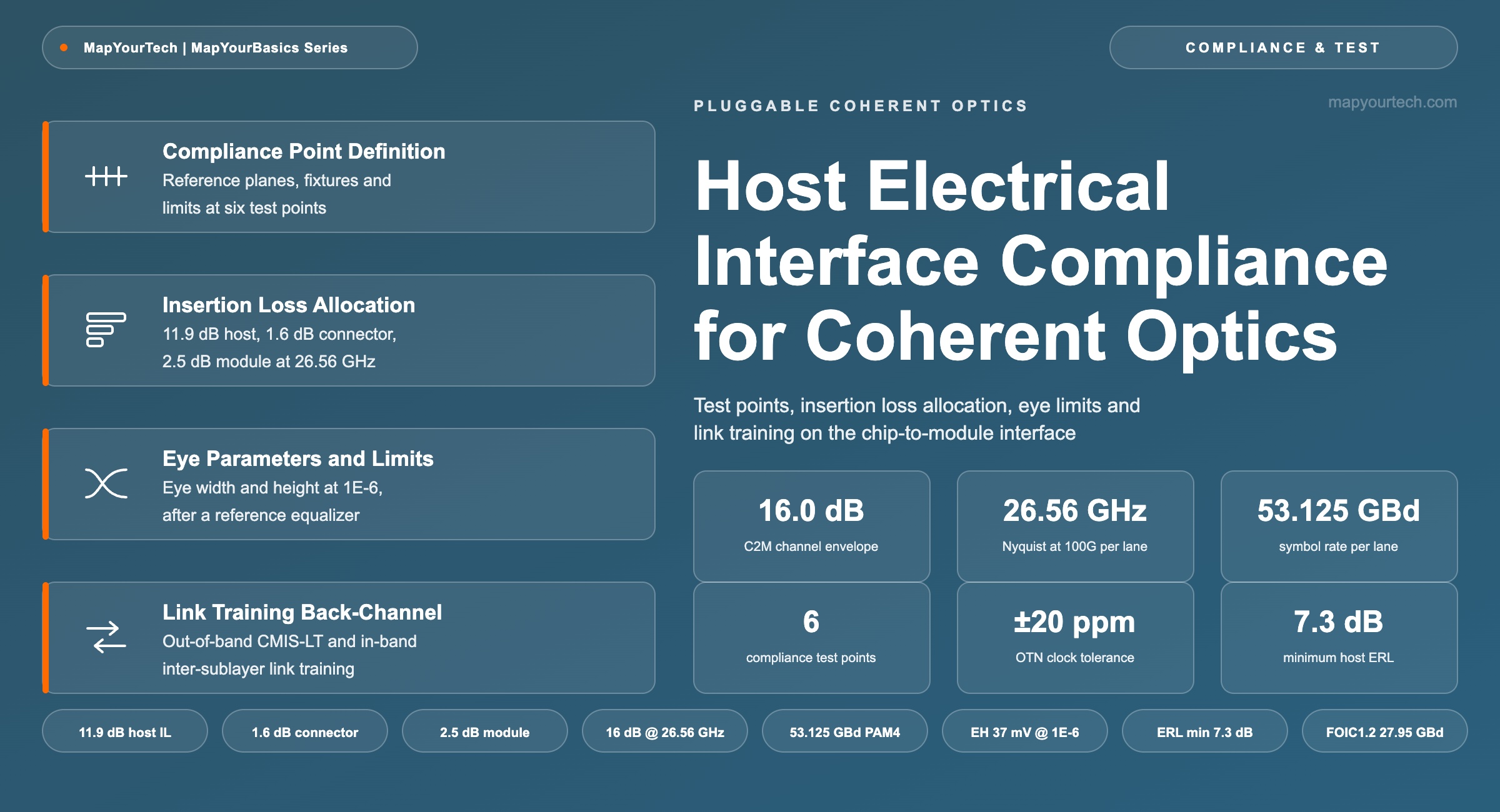
Host Electrical Interface Compliance for Pluggable Coherent Optics
Test points, insertion loss allocation, eye limits, link training and client mapping across the short electrical channel between a router ASIC and a coherent module DSP.
Two vendors agree on the reference point or they agree on nothing.
1. Introduction
Between a router or switch application-specific integrated circuit (ASIC) and the coherent digital signal processor (DSP) inside a pluggable module sits a short electrical channel: a few inches of printed circuit board, one pluggable connector, and a stub of module board. That channel carries the full port rate, and it has its own budget, its own compliance points, and its own conformance suite. A module that meets every optical parameter in an 800ZR Implementation Agreement will still fail to bring a port up if the host board loses more than its allocation at the Nyquist frequency of the lane rate, if the connector footprint pushes return loss below the specified floor, or if the host requests a client configuration the module does not advertise.
The framework governing that channel is the Attachment Unit Interface (AUI) chip-to-module interface (C2M) in IEEE 802.3, and the very short reach (VSR) interface in the Optical Internetworking Forum (OIF) Common Electrical I/O (CEI) family. Both describe the same arrangement and share a test methodology deliberately: a loss allocation split between host and module board, near-end measurement through compliance boards, eye limits evaluated at a stated error probability after a reference equalizer, and a return loss floor at each interface. Above it sits the Common Management Interface Specification (CMIS), which decides which host lane configurations a module will accept and carries the path by which a module asks the host to retune its transmitter.
This overview maps that framework end to end: where the compliance points sit, how the loss budget is divided, what the eye parameters mean in practice, how the back-channel operates, and how gearbox and lane-mapping choices determine which client mixes a port supports.
2. Compliance Point Definition and Reference Planes
A compliance point is a defined reference plane in the electrical channel between a host board and a pluggable module, at which signal parameters are specified, measured and accepted. Each compliance point fixes one physical location, one measurement fixture and one limit set, so that a host and a module qualified independently will interoperate when mated.
Four neighbouring quantities are routinely conflated at this boundary. A compliance point is a location in the channel, while a compliance board is the calibrated fixture used to reach that location, and the two carry separate names because one host output can be measured through more than one fixture. A near-end limit applies to a signal measured close to its source through a compliance board, while a far-end limit applies to that same signal after it has crossed the reference test channel. TP1a and TP1 sit on opposite faces of one mated connector, so a host output measured at TP1a and a module input specified at TP1 differ by the connector and the module board between them. Insertion loss and return loss are both specified at compliance points and describe different things: insertion loss is the power the channel removes on the way through, and return loss is the power it sends back toward the source.
Channel Loss Between Compliance Points
IL(fN) = ILhost + ILconnector + ILmodule, evaluated at fN = Rb / 4
Where:
- IL — insertion loss in dB, for the channel element named in the subscript.
- fN — Nyquist frequency in GHz, the single point on the frequency axis at which every loss limit is stated.
- Rb — lane bit rate in Gb/s; the divisor is 4 because four-level pulse amplitude modulation (PAM4) carries two bits per symbol and the Nyquist frequency is half the symbol rate.
Take a 106.25 Gb/s lane. It runs at 53.125 GBd, so fN = 106.25 / 4 = 26.5625 GHz. At that frequency the chip-to-module allocation is 11.9 dB across the host, 1.6 dB across the connector and 2.5 dB across the module, which sum to 16.0 dB between TP0 and TP5 (standard-specified, IEEE 802.3 chip-to-module allocation). Every eye, return-loss and training limit quoted below applies to that same lane at that same frequency.
Takeaway: A compliance point names a location, a fixture and a limit set together, and a measurement quoted without all three is unusable, because the same lane can pass at one point and fail at the next.
3. Test Points and Compliance Boards
Neither the host ASIC output nor the module DSP input can be probed once a line card is assembled, so every compliance point is reached through a fixture instead. A host compliance board (HCB) presents the module face of the connector to a host under test, and a module compliance board (MCB) presents the host face to a module under test, each with calibrated impedance and known loss. Those two fixtures are what let a host vendor qualify a board that will never meet the module it eventually carries.
Six test points describe a bidirectional lane. On the host-to-module path, TP0 is the host ASIC serializer/deserializer (SerDes) output at the package, TP1a is the host output measured at the connector through an HCB, and TP1 is the module input. On the module-to-host path, TP4 is the module output measured through an MCB, TP4a is the host input reference, and TP5 is the host receiver input.
The interface is not designed to be error free on its own. IEEE 802.3ck evaluates a chip-to-module link at a pre-forward-error-correction (pre-FEC) bit error ratio of 1 × 10⁻⁵, while the OIF very short reach clause works to 1 × 10⁻⁶ (vendor specification summarising both frameworks). The Reed-Solomon RS(544,514) code in the Ethernet physical coding sublayer then brings the link to a post-FEC bit error ratio at or below 1 × 10⁻¹⁵ at the media access control service interface (vendor specification). Which target a measurement was taken at matters: a lane at 3 × 10⁻⁶ is compliant for Ethernet and out of specification for an Optical Transport Network (OTN) client on the same connector.
| Test point | Location | What is measured |
|---|---|---|
| TP0 | Host ASIC output at the package | Reference for the host transmitter before the board channel; not accessible in an assembled product |
| TP1a | Host output at the connector, through an HCB | Near-end host transmitter output: eye width, eye height, vertical eye closure, return loss, common-mode noise |
| TP1 | Module input at the module connector | Far-end signal presented to the module receiver, and the stressed input used to qualify module receiver tolerance |
| TP4 | Module output at the connector, through an MCB | Near-end module transmitter output, same parameter set as TP1a with module limits |
| TP4a | Host input reference at the connector | Far-end reference for the module output after the host channel |
| TP5 | Host receiver input at the ASIC package | Reference for the host receiver; qualified by simulation and by the stressed input test at TP4a |
Takeaway: Host and module are qualified separately against the same test-point definitions, so an integration failure is normally traceable to one side exceeding its own allocation rather than to an interaction that only appears when the two are mated.
4. Insertion Loss Allocation and Nyquist Frequency
Insertion loss is specified at the Nyquist frequency because that is where a lossy channel takes most of the amplitude out of a PAM4 eye, and the frequency follows the symbol rate rather than the bit rate. Three lane generations put it at three different places on the frequency axis, and each generation carries its own allocation.
Nyquist Frequency of a PAM4 Lane
fN = Rs / 2 = Rb / (2 · log2M) = Rb / 4
Where:
- fN — Nyquist frequency in GHz; the point at which channel insertion loss is specified. Typical values 13.28–53.125 GHz.
- Rs — symbol rate in GBd. Typical values 26.5625, 53.125 and 106.25 GBd.
- Rb — lane bit rate in Gb/s. Typical values 53.125, 106.25 and 212.5 Gb/s.
- M — modulation levels; 4 for PAM4, so log2M = 2.
Worked value: a 106.25 Gb/s lane gives Rs = 53.125 GBd and fN = 26.5625 GHz. Halving the lane rate to 53.125 Gb/s gives 26.5625 GBd and 13.28125 GHz; doubling it to 212.5 Gb/s gives 106.25 GBd and 53.125 GHz.
IEEE 802.3ck divides the 100 Gb/s per lane chip-to-module channel into three named shares at 26.56 GHz: up to 11.9 dB for the host, up to 1.6 dB for the host connector, and up to 2.5 dB for the module (standard-specified, IEEE 802.3 chip-to-module allocation). The OIF states the same envelope from the other direction: CEI-112G-VSR-PAM4 covers 36–58 GBd with up to 16 dB of loss at the Nyquist frequency including one connector, and hosts and modules built to it by different manufacturers are expected to interoperate (standard-specified, OIF).
Those figures translate into board length. Task force contributions put differential trace loss at 1.24 dB per inch on one low-loss laminate and 1.64 dB per inch on a higher-loss laminate, both at 28 GHz, with roughly 0.5 dB per footprint via. Against a 7 dB printed-circuit-board share of the host allocation, that allows under about 5 inches of trace on the low-loss material and under about 4 inches on the higher-loss one. Front-panel channels on the outer ports of a fixed switch run 12–14 inches, which is why cabled fly-over assemblies appear between the ASIC and the edge cages (industry contribution).
Doubling the lane rate rewrote the whole budget. One coherent module specification allocates 6.2 dB to the host at 13–14 GHz and 4.0 dB inside the module at 50 Gb/s per lane, against 10.0 dB to the host at 26.56–28 GHz and 6.0 dB inside the module at 100 Gb/s per lane, with the receive equalizer designed to recover about 10.2 dB at 14 GHz and about 16.0 dB at 28 GHz (vendor specification). The equalizer, not the copper, absorbed the change.
| Generation | Lane bit rate | Symbol rate | Nyquist | Chip-to-module framework | Channel envelope |
|---|---|---|---|---|---|
| 50 Gb/s per lane | 53.125 Gb/s | 26.5625 GBd | 13.28 GHz | IEEE 802.3bs and 802.3cd C2M; OIF CEI-56G-VSR-PAM4 | ~10.2 dB |
| 100 Gb/s per lane | 106.25 Gb/s | 53.125 GBd | 26.56 GHz | IEEE 802.3ck C2M; OIF CEI-112G-VSR-PAM4 | 16.0 dB |
| 200 Gb/s per lane | 212.5 Gb/s | 106.25 GBd | 53.125 GHz | IEEE P802.3dj C2M; OIF CEI-224G-VSR | In ballot |
At 50 Gb/s per lane the envelope came from separate host and module tables rather than from one channel figure, so the value above is a vendor specification rather than a published channel number. At 100 Gb/s per lane it is the sum of the three standard-specified shares. At 200 Gb/s per lane no channel figure is fixed yet, because the IEEE draft is in ballot.
Practical Example — checking a host board against the allocation
A line card places its coherent cage 4.2 inches from the ASIC on a laminate measured at 1.24 dB/in at 28 GHz. Trace loss is 4.2 × 1.24 = 5.2 dB, and two footprint vias at 0.5 dB each add 1.0 dB, giving 6.2 dB of board loss. Adding a 1.6 dB connector and a 2.5 dB module share brings the mated channel to 10.3 dB at 26.56 GHz, inside the 16.0 dB envelope with margin. The same geometry at 200 Gb/s per lane loses far more, because trace and via loss both increase with frequency, which is why cabled assemblies and shorter host channels replaced the attempt to hold one board layout at twice the Nyquist frequency.
Takeaway: The host owns roughly three-quarters of the chip-to-module loss budget, so cage placement and laminate choice on the host board decide whether a coherent port works long before the module is selected.
5. Eye Parameters and the Reference Receiver
Eye width and eye height on a chip-to-module interface are stated at a probability, not as an absolute opening, because the eye at 100 Gb/s per lane is closed at the pin and only opens inside the receiver. The measurement is taken on a statistical contour at a probability of 1 × 10⁻⁶ after a reference receiver, so random jitter and noise are included on the same terms for every implementation. The reference receiver adopted for the 100 Gb/s per lane chip-to-module interface is a continuous-time linear equalizer followed by a four-tap decision feedback equalizer, with the first tap magnitude limited to 0.5 and taps two to four limited to 0.2, and with the adaptation algorithm specified explicitly so that two laboratories measuring the same board reach the same number (task force baseline).
Eye width is the horizontal opening in unit intervals (UI). Eye height is the vertical opening in millivolts, evaluated on the upper, middle and lower PAM4 eyes separately because they are not identical. Vertical eye closure states in dB how much transmitted amplitude the channel and the transmitter have taken away, and it catches a transmitter whose equalizer settings look valid but have overdriven the pre-cursor.
| Parameter | Compliance point | 53–56 GBd | 106–112 GBd |
|---|---|---|---|
| Eye width, minimum | Near end at TP4 | 0.265 UI | 0.200 UI |
| Eye height, minimum | Near end at TP4 | 70 mV | 37 mV |
| Eye width, minimum | Far end | 0.200 UI | 0.150 UI |
| Eye height, minimum | Far end | 30 mV | 15 mV |
| Differential output, peak to peak | Near end at TP4 | 900 mV | 900 mV |
| Loss compensated by receive equalizer | Module receiver | 10.2 dB | 16.0 dB |
These are vendor specification values for one coherent pluggable implementation, quoted at the stricter 1 × 10⁻⁶ probability so they hold for both Ethernet and OTN use. Doubling the lane rate halves the far-end eye height and takes a quarter off the far-end eye width, and the receive equalizer has to recover what remains.
Return loss carries its own floor. IEEE 802.3ck sets a minimum effective return loss of 7.3 dB at the chip-to-module host, 8.5 dB at the module, and 10.3 dB at the mated test fixture (standard-specified, IEEE 802.3). Effective return loss folds the reflection into a single figure of merit weighted by where in the pulse response the reflection lands, which is why a connector footprint that looks acceptable on a raw S-parameter plot can still fail. Receiver tolerance is qualified separately by a stressed input test: a calibrated impaired signal is applied at TP1 for the module input and at TP4a for the host input, and the receiver has to hold the target error ratio while it is applied.
Measurement note
Near-end and far-end limits are not interchangeable. A module output meeting the near-end eye height at TP4 was measured through a module compliance board only, while the far-end limit assumes the full reference test channel has been crossed. Comparing a near-end measurement against a far-end limit is the most common way a compliant board is recorded as failing.
Takeaway: The eye is specified statistically after a defined equalizer, so a chip-to-module measurement is only meaningful when the probability, the compliance point and the reference receiver settings are all stated with it.
6. Link Training and the Host Transmitter Back-Channel
A host transmitter equalizer set at manufacturing cannot cover the range of channels a pluggable cage will see, so the module is given a path to ask the host to retune. Board-to-board variation, cage position along the faceplate, temperature and aging all move the channel, and at 11.9 dB of host loss the difference between a good tap set and an adequate one shows up in the pre-FEC error ratio. The back-channel closes that loop: the receive digital signal processor inside the module reads its own recovered signal and asks the host to increment, decrement or hold each feed-forward equalizer (FFE) coefficient.
The out-of-band path is defined by the OIF as CMIS for out-of-band link training, used alongside the Common Management Interface Specification. It is protocol agnostic, runs over the two-wire management interface rather than the data lanes, and can be engaged on egress, ingress or both. It reaches up to seven pre-cursor and eight post-cursor taps, supports selectable step sizes, and lets a host store an optimised preset and reapply it after a reset instead of converging from zero. Its stated use cases span OIF CEI-112G, IEEE 802.3ck, Fibre Channel, InfiniBand and CEI-224G (standard-specified, OIF project scope).
The in-band path sits inside Ethernet itself. IEEE P802.3dj defines inter-sublayer link training, which exchanges training frames on the data lanes before the interface enters data mode, and makes it mandatory for 200 Gb/s per lane Ethernet physical layers and attachment unit interfaces (standards-body draft). Above it sits autonomous path start-up, which brings an end-to-end path up without host intervention at each hop. An OIF CMIS supplement defines the registers a host uses to manage host-side and media-side training on a CMIS module, so both mechanisms are managed through one interface.
Practical Example — a port that comes up but reports a poor error ratio
A 400G coherent port links and passes traffic, but the module reports a pre-FEC bit error ratio near 2 × 10⁻⁴ on two of eight lanes while the other six sit near 1 × 10⁻⁶. Because the fault is per lane rather than per port, the optical side is not implicated: an optical impairment moves every lane together after the DSP. The two affected lanes are the longest routes on the board, and the fix is normally a training pass rather than a hardware change. Reading back the host transmit taps before and after training shows whether the host applied the module's requests.
Takeaway: Per-lane error ratio differences on an otherwise healthy port point at the electrical channel and its equalizer settings, and the back-channel is the mechanism that resolves them without touching the board.
7. Lane Mapping, Gearboxes and Permitted Client Mixes
A coherent module accepts only the host lane configurations it advertises, and that list decides whether a given line card and module will form a port. An 800 Gb/s coherent module built to the OIF implementation agreement presents its host side as one 800GAUI-8, two 400GAUI-4, four 200GAUI-2 or eight 100GAUI-1 interfaces, carrying Ethernet clients down to 100GE (standard-specified, OIF 800ZR). The module DSP gearboxes between whichever structure the host uses and its own internal rate, so one module serves a host with eight 100 Gb/s lanes and a host with four 200 Gb/s lanes alike.
CMIS turns that flexibility into something a host can discover. An application pairs a standard host electrical interface identifier with a standard media interface identifier, and the application selection code is one numeric value representing that pair. Both identifiers are registered in the SFF module management reference code tables, and a module publishes the applications it supports. A host may select an advertised application and nothing else, so a configuration that looks reasonable on paper fails to apply if the module does not carry it. For QSFP-DD or OSFP coherent optics, that table comes ahead of any optical planning.
OTN clients change the electrical picture in two ways. The Flexible OTN (FlexO) interface rates defined in ITU-T G.709.1 run above the equivalent Ethernet rates, so a host lane carrying an OTN client runs at a different symbol rate from the same lane carrying Ethernet. The clock tolerance also tightens, from ±100 ppm for Ethernet to ±20 ppm for the OTN interfaces. A host SerDes that supports only the Ethernet rate cannot present an OTN client to the module at all, regardless of what the optical side can do — a constraint that shapes IP over DWDM designs where OTN handoff is still required.
OTN Lane Symbol Rate Relative to Ethernet
Rs,OTN = Rs,ETH × k, with k = 1.0523
Where:
- Rs,ETH — Ethernet lane symbol rate in GBd at ±100 ppm. 26.5625 GBd for 50 Gb/s per lane, 53.125 GBd for 100 Gb/s per lane.
- Rs,OTN — FlexO interface lane symbol rate in GBd at ±20 ppm.
- k — rate ratio, derived from the published FlexO and Ethernet rates. Value 1.0523, an increase of about 5.23%.
Worked value: 26.5625 × 1.0523 = 27.952 GBd, which matches the published FOIC1.2 lane rate of 27.95236 GBd. At the higher lane rate, 53.125 × 1.0523 = 55.905 GBd, matching the published FOIC1.1 lane rate of 55.90473 GBd. Both are standard-specified values; the ratio is derived from them.
| Client on the host interface | Lane symbol rate | Clock tolerance | Physical coding |
|---|---|---|---|
| Ethernet at 50 Gb/s per lane | 26.5625 GBd | ±100 ppm | PAM4 with RS(544,514) |
| Ethernet at 100 Gb/s per lane | 53.125 GBd | ±100 ppm | PAM4 with RS(544,514) |
| FlexO interface FOIC1.2 | 27.95236 GBd | ±20 ppm | PAM4 with RS(544,514) |
| FlexO interface FOIC1.1 | 55.90473 GBd | ±20 ppm | PAM4 with RS(544,514) |
| OTU4 over OTL4.2 | 27.95249 GBd | ±20 ppm | PAM4 with RS(255,239) |
The Ethernet rates are fixed by IEEE 802.3 and the FlexO and OTL rates by the ITU-T Recommendations, so all of them are standard-specified. An OTN-capable port needs host silicon that can retune both its SerDes and its reference clock, and a port designed only for Ethernet clients cannot be turned into an OTN port by firmware. Where OTN wrapping is not required, that constraint disappears.
Takeaway: Lane count, lane rate and clock tolerance together define what a port can carry; the module's advertised application table is the authoritative list, and it is discoverable before deployment.
8. Standards Framework and Interoperability
IEEE 802.3, the OIF and ITU-T Study Group 15 divide this framework between them and align deliberately rather than competing. IEEE 802.3 specifies the chip-to-module and chip-to-chip attachment unit interfaces for Ethernet, with the 100 Gb/s per lane interfaces defined as 100GAUI-1, 200GAUI-2 and 400GAUI-4. The OIF specifies the same channel as CEI-112G-VSR-PAM4, covering 36–58 GBd with up to 16 dB at the Nyquist frequency including one connector, and reuses the IEEE test setup so a single laboratory configuration serves both (standard-specified, OIF). The OIF also owns the management layer: CMIS for the core register model, Coherent CMIS for digital coherent optics, and supplements for link training, firmware update and security. ITU-T Study Group 15 defines the FlexO interfaces that carry OTN clients across the same connector.
Interoperability is verified in public. OIF multi-vendor demonstrations at OFC and ECOC exercise very short reach channels across silicon from different suppliers. One ran 212.5 Gb/s PAM4 across a die-to-die channel with 32 dB of insertion loss at 56 GHz, alongside a second channel emulating a switch-ASIC-to-faceplate path terminated in a mated module compliance board (forum demonstration). An earlier one ran the first multi-vendor 224G interoperability over a test board with 29 dB of die-to-die insertion loss. These events stress the compliance board methodology against real silicon rather than against models.
Coherent module and DSP vendors publish host electrical tables that state the supported attachment unit interfaces, the per-lane rates, the compliance points and the loss allocated inside the module. Those tables are the working interoperability contract for a hardware engineer, alongside the pluggable nomenclature that names the interfaces and the form factor specifications that fix the connector and cage.
Takeaway: The electrical interface has one physical definition shared across IEEE and OIF documents, one management model in CMIS, and one place where OTN diverges from Ethernet, which is the lane rate.
9. Evolution to 200 Gb/s per Lane
The next generation moves the Nyquist frequency to 53.125 GHz, and the compliance framework changes with it. IEEE P802.3dj defines 200 Gb/s per lane electrical interfaces alongside 200GbE through 1.6TbE, is in Standards Association ballot, and its task force timeline targets completion later in 2026 (standards-body timeline). For host designers the visible change is that inter-sublayer link training becomes mandatory, because at 53 GHz a factory-set transmitter tap vector no longer covers the channel population.
The OIF is building the matching implementation agreements. CEI-224G-VSR states a reach objective of at least 200 mm of host channel, 20 mm of module channel and up to one connector over advanced materials, while CEI-224G-Linear defines behaviour at TP1, TP1a, TP4 and TP4a for modules with no retimer. A separate protocol-agnostic link training agreement for 224G PAM4 covers messaging format, training patterns, state sequences and fault handling. CEI-448G-VSR is already open with the same 200 mm host and 20 mm module objective, so the host channel is not expected to grow.
The line side moves in parallel. OIF projects for 1600ZR and 1600ZR+ define the coherent interfaces that will sit behind those host lanes, with 1600ZR+ built around a fixed hierarchical tree physical coding sublayer, open forward error correction, dual-polarization 16-state quadrature amplitude modulation (DP-16QAM) and two digital subcarriers. A 1.6 Tb/s coherent module is deployable only where the host board can deliver 200 Gb/s per lane to its connector, which binds the electrical and optical halves of the pluggable roadmap to one schedule.
Takeaway: At 200 Gb/s per lane the host channel stops growing and the equalizer and training mechanisms take over, which shifts integration effort from board layout toward configuration and management.
10. Conclusion
The electrical channel between a router ASIC and a coherent module DSP is short, and it is fully specified. Six compliance points define where measurements are taken, three named shares divide the insertion loss at the Nyquist frequency, eye width and eye height are stated on a probability contour after a defined reference receiver, a return loss floor applies at each interface, and a back-channel tunes the host transmitter after the board is built. None of that appears in an optical link budget, and all of it decides whether a coherent port comes up.
Three decisions carry most of the risk on a line card. Cage distance from the ASIC and laminate choice together set whether the design fits the host share of the budget at the Nyquist frequency of the intended lane rate. The module's advertised host electrical interfaces have to include one the host silicon can drive. And OTN clients require a host SerDes that runs at the FlexO rate with ±20 ppm tolerance. Settling those three before layout costs a design review; settling them afterwards costs a respin, because the optical side of a coherent deployment and the FEC that protects it both assume this channel is already sound.
11. References
- IEEE Std 802.3ck, Physical Layer Specifications and Management Parameters for 100 Gb/s, 200 Gb/s, and 400 Gb/s Electrical Interfaces Based on 100 Gb/s Signaling, IEEE Standards Association.
- IEEE P802.3dj, 200 Gb/s, 400 Gb/s, 800 Gb/s, and 1.6 Tb/s Ethernet, IEEE 802.3 Ethernet Working Group.
- Optical Internetworking Forum, Common Electrical I/O Implementation Agreement — CEI-112G-VSR-PAM4 Very Short Reach Interface, OIF.
- Optical Internetworking Forum, Common Management Interface Specification (CMIS), OIF.
- Optical Internetworking Forum, CMIS for Out-of-Band Link Training (CMIS-LT), OIF.
- Optical Internetworking Forum, Implementation Agreement for 800ZR, OIF.
- ITU-T Recommendation G.709.1/Y.1331.1, Flexible OTN Short-Reach Interface, ITU-T Study Group 15.
- SNIA SFF-8024, SFF Module Management Reference Code Tables, SNIA SFF Technology Affiliate.
- Sanjay Yadav, "Optical Network Communications: An Engineer's Perspective" — Bridge the Gap Between Theory and Practice in Optical Networking.
Related Articles on MapYourTech