Host Power and Thermal Design for Coherent Pluggables
An application note on the power and thermal contract a line card owes a high-power coherent module: rail tolerance, contact current ceilings, inrush limiting, removal interlocks, and per-die temperature limits.
The parameter nobody owns is the parameter that fails.
1. Introduction
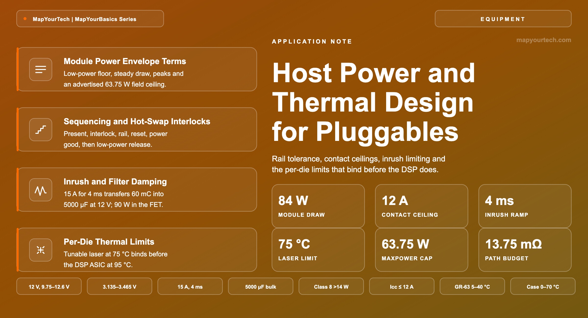
A high-power flexrate coherent module in a 192-contact embedded form factor draws up to 84 W from a single 12 V rail, holds 5000 µF of bulk capacitance behind its input pins, limits its own low-power state to 30 W, and releases traffic only after the host has driven module-present, reset, power-good and low-power in a fixed order (vendor specification, representative 1.2 Tb/s-class embedded module). The 84 W is the number that reaches the rack power spreadsheet. The 5000 µF, the 15 A inrush ceiling and the 75 °C long-term limit on the tunable laser are the numbers that decide whether the module runs at all.
Rack-level power arithmetic follows from the module datasheet figure, and MapYourTech works it through in the power-per-bit analysis of router optics and in the wider energy-efficiency treatment of pJ/bit metrics. This note covers the other side of the interface: what the line card has to provide, in what order, and with what margin, before the module reaches its ready state.
Two hardware families share the same set of problems and solve them with different pin counts. Front-panel pluggables in the QSFP-DD and OSFP families run from a 3.3 V rail distributed across several contacts, advertise their power appetite through the Common Management Interface Specification (CMIS), and depend on a low-power boot state to protect a host that cannot feed them. Embedded flexrate modules run from a 12 V rail with a dedicated hot-swap controller, mechanical interlocks and vendor-defined control lines. The design method is common to both: bound the current, damp the input network, sequence the control lines, and treat the reported die temperatures rather than the case temperature as the thermal contract.
Every number quoted here carries its source class. Standard-specified values come from CMIS, the QSFP-DD MSA hardware specification, the OSFP MSA module specification and Telcordia GR-63-CORE. Vendor specification values come from a representative high-power embedded coherent module. Computed values are derived in the text from those inputs and are labelled as such.
The host-side electrical and thermal contract is the subject here. Optical performance, framing and the coherent digital signal processing (DSP) datapath sit instead in the MapYourTech treatments of 800ZR and 800ZR+ coherent pluggables and coherent versus direct-detect application boundaries.
2. Module Power Envelope Definition and Component Terms
A module power envelope is the ordered set of electrical demands a pluggable places on its host: a low-power floor, a steady-state operating draw, a sustained peak, an instantaneous peak, and an advertised maximum that bounds them all. Each term is a power in watts, and each maps to a current through the rail that supplies it.
The five terms separate in time as well as in magnitude. The low-power floor holds from the moment the rail is established until the host releases low power, the instantaneous peak lasts tens of microseconds during a state transition, and the steady-state draw persists for the service life of the module. A supply sized on any single term meets the specification at one point in that sequence and misses it at another.
Five pairs of adjacent quantities account for most of the confusion in host power budgets, and each pair separates on a single property.
- Advertised maximum against steady-state draw. The advertised figure is a permission ceiling the host has to be able to supply, while the steady-state draw is what the module takes in its present configuration, and the two diverge whenever a module runs below its highest line rate.
- Power against rail current. The module specification bounds power and the connector specification bounds current, with only the bus voltage linking them, so a 25 W module is a 7.6 A load on a 3.3 V rail and a 2.1 A load on a 12 V rail (both computed).
- Instantaneous peak against sustained peak against steady-state ceiling. The instantaneous peak is bounded over a 50 µs window, the sustained peak over a longer transition, and the steady-state ceiling over the service life, which is why all three appear in the same specification table with different values (standard-specified, QSFP-DD MSA).
- Low-power floor against off. A module held in low power is energised, initialised and answering management reads, so the floor is a load the slot budget carries rather than a saving that appears when a port sits idle.
- Module power against slot power. The slot draws the module figure plus host conversion loss and the share of the fan power the module's dissipation calls for, so a rack budget assembled from module datasheet figures alone understates the shelf.
I = PVbus Padvertised = 0.25 W × N201
- I — current drawn through the supply rail, in amperes.
- P — the envelope term being converted, in watts. Any of the five terms above.
- Vbus — nominal bus voltage, in volts. 3.3 V for front-panel pluggables, 12 V for embedded modules.
- N201 — the unsigned count held in CMIS Page 00h byte 201, range 0–255, giving 0–63.75 W in 0.25 W steps.
A representative high-power flexrate module states a 30 W low-power state, an 84 W operating maximum, a 9 A input current rating and a 15 A inrush ceiling on a 12 V rail (vendor specification). Converting each term through Formula 1 gives 2.5 A in low power, 7.0 A in operation, 108 W at the rated input current and 180 W instantaneous during inrush (all computed). The spread between the smallest and largest term is a factor of six in current, and every one of those numbers lands on a different part of the host design: the low-power figure sizes the boot budget, the operating figure sizes the copper, the rated current sizes the protection threshold, and the inrush figure sizes the hot-swap pass element. The advertised maximum has no representation at all here, because 84 W exceeds the 63.75 W ceiling of the CMIS field, which is why this class carries a vendor-defined power contract alongside the management interface.
Takeaway: Module power is five numbers, not one, and they separate by time window as well as by magnitude. Every section that follows works on one of the five, so a host budget that collapses them into a single wattage has already lost the distinction the rest of the design depends on.
3. Technical Background
A host that powers a module before knowing what the module will draw has already lost the argument. CMIS resolves this with an advertisement-then-permission model: the module boots into a state that draws almost nothing, publishes what it needs, and waits for the host to allow the transition. The hardware specifications behind each form factor then bound how much current the connector and the host filter can deliver, and the environmental standards bound the ambient conditions under which those limits have to hold.
3.1 Power Classes and MaxPower Advertising
CMIS carries the module's power appetite in two adjacent bytes of Page 00h. Byte 200 holds the power class in its upper three bits, and byte 201 holds the maximum power consumption in units of 0.25 W (standard-specified, CMIS). The QSFP-DD MSA hardware specification fixes eight classes at 1.5, 3.5, 7, 8, 10, 12, 14 W and, for class 8, any value above 14 W (standard-specified, QSFP-DD MSA). A module that reports class 8 obliges the host to read byte 201, because the class alone no longer states a number.
The 0.25 W granularity sets a ceiling of its own. One byte at 0.25 W per count reaches 63.75 W (computed), so the CMIS MaxPower field can describe any module up to that figure and nothing beyond it. That is comfortably above where front-panel coherent pluggables sit today and comfortably below the 84 W of the embedded flexrate class, which is one reason the embedded family keeps its own vendor-defined power contract rather than relying on the CMIS advertisement alone.
| Power class | Max power (W) | Instantaneous peak (mA) | Sustained peak (mA) | CMIS advertisement |
|---|---|---|---|---|
| Class 1 (low power) | 1.5 | 600 | 495 | Byte 200, bits 7:5 |
| Class 2 | 3.5 | 1400 | 1155 | Byte 200, bits 7:5 |
| Class 3 | 7.0 | 2800 | 2310 | Byte 200, bits 7:5 |
| Class 4 | 8.0 | 3200 | 2640 | Byte 200, bits 7:5 |
| Class 5 | 10.0 | 4000 | 3300 | Byte 200, bits 7:5 |
| Class 6 | 12.0 | 4800 | 3960 | Byte 200, bits 7:5 |
| Class 7 | 14.0 | 5600 | 4620 | Byte 200, bits 7:5 |
| Class 8 | above 14 | P/2.5 A | P/3.03 A | Byte 201, 0.25 W steps |
Instantaneous and sustained peak currents are not the operating current, and they are the pair most often skipped in host budgets. They bound the envelope the host filter network has to absorb during state transitions, measured as the combined current through all inductors in the host filter (standard-specified, QSFP-DD MSA). For class 8 the peaks scale with the advertised power, and a separate steady-state ceiling of 12 A applies regardless of the advertised figure.
3.2 Module State Machine and Power Mode Control
CMIS defines a module state machine whose states the host reads directly: MgmtInit, ModuleLowPwr, ModulePwrUp, ModuleReady, ModulePwrDn and ModuleFault (standard-specified, CMIS). Management initialisation completes within 2000 ms of power-on, hot plug or the rising edge of reset, measured to the first acknowledged transaction on the two-wire interface (standard-specified, QSFP-DD MSA). After that the path forks on the module's init mode. In software init mode the module rests in ModuleLowPwr and waits; in hardware init mode it advances to ModulePwrUp without host management action.
Three controls decide which way the module goes. The LPMode hardware pin, asserted high by the host at hot plug, power cycle or reset, holds the module in low power mode; released low, the module proceeds to high power mode with no management intervention at all (standard-specified, QSFP-DD MSA). Lower Memory byte 26 carries the two software equivalents, LowPwrRequestSW and LowPwrAllowRequestHW, the second of which decides whether the module evaluates the hardware pin at all (standard-specified, CMIS). A host that pulls LPMode low on a board whose power budget cannot carry a class 8 module has removed its own protection.
Assert LPMode before applying power and hold it until the host has read byte 200, read byte 201 where the class is 8, and confirmed that the slot budget covers the advertised figure. Releasing LPMode is the host's statement that it can feed and cool the module, and the module treats it as such.
3.3 Supply Rails and Contact Current Ceilings
Front-panel modules take 3.3 V across six power contacts: VccTx, VccTx1, VccRx, VccRx1, Vcc1 and Vcc2, applied concurrently, with a permitted range of 3.135–3.465 V including ripple, droop and noise below 100 kHz (standard-specified, QSFP-DD MSA). Each Vcc contact is rated for 2000 mA steady state and each ground contact for 500 mA. Multiply the contact rating by the contact count and the electrical ceiling appears: six contacts at 2 A give 12 A (computed), which is exactly the steady-state limit the specification states for class 8. At the 3.3 V nominal that is 39.6 W, and at the 3.135 V floor it is 37.6 W (computed).
That arithmetic explains why front-panel form factors have converged on roughly 40 W as their electrical horizon, and why the QSFP-DD1600 variant lifts contact ratings to 2 A with a stated feasibility of at least 40 W of module dissipation (standard-specified, QSFP-DD MSA). It also explains the specification note that for class 4 and above the module's differential loading of the input pads must not push any single contact past its rating. A module that draws its whole load through two of six pads meets the total-current limit and still overheats a contact.
Two further rail requirements shape the host filter. The module has to tolerate supply variations with a slew rate up to 175 mV/ms without traffic hits or two-wire errors, and the noise budget is split three ways: the host may emit no more than 25 mV RMS integrated from 40 Hz to 10 MHz, the module no more than 30 mV RMS over the same band, and the module has to keep operating with a 66 mV peak-to-peak sinusoidal noise tolerance applied at its pads (all standard-specified, QSFP-DD MSA). Voltage lost across the host filter counts against the host's DC set-point accuracy, so filter component resistance is a budget item rather than a detail.
OSFP takes the same 3.3 V approach with four Vcc contacts and combines functions on its low-speed pins: LPWn/PRSn carries low-power request and module presence on one multi-level line, and INT/RSTn carries interrupt and reset on another (standard-specified, OSFP MSA). The mating order is identical in both families and in the embedded form factor: ground first, power second, signals third, with de-mating in reverse. That sequencing is what protects the signal pins from carrying inrush current during insertion. The trade-offs between the two front-panel families are set out in the MapYourTech guide to pluggable nomenclature and form factor selection and in the QSFP-DD transceiver overview.
3.4 Twelve-Volt Embedded Modules
Above about 40 W the 3.3 V rail stops making sense. An 84 W module on 3.3 V would draw 25.5 A; on 12 V it draws 7.0 A (computed). The embedded flexrate class therefore runs from a single 12 V supply with an input range of 9.75–12.6 V inclusive of ripple, a supply ripple limit of 1% from 1 kHz to 20 MHz, an input current rating of 9 A, undervoltage lockout on the module side, and 5000 µF of low-ESR bulk capacitance inside the module (vendor specification, representative embedded module). The low-power state draws 30 W, a little over a third of the 84 W operating figure rather than the near-zero of a CMIS class 1 boot.
Undervoltage lockout is the mechanism that turns a marginal host design into an intermittent one. The module trips its lockout when the 12 V rail sits below threshold for a defined interval, so a host operating near the 9.75 V floor with insufficient decoupling will meet the DC specification on a meter and still fail to pass traffic, because the transient excursions during DSP state changes cross the threshold. High capacitance with low equivalent series inductance near the connector is the stated remedy, not a larger bulk capacitor further away.
Takeaway: The advertised power figure is a permission request, not a design input. The design inputs are the contact current rating, the rail tolerance window, the noise budget and the transition-peak envelope, and each of those is fixed by the form factor rather than by the module.
4. Application Description
A line card carrying several coherent modules commits a large fraction of its slot budget to the pluggables alone. Router and transport chassis meet the same problem, and its chassis-level consequences are set out in the MapYourTech IP over DWDM primer. Three behaviours decide whether that line card works in the field rather than only on the bench: the order in which the host brings the module up, the order in which it takes the module down, and what it does with the temperatures the module reports while running.
4.1 Insertion and Power-Up Sequencing
Insertion is mechanical before it is electrical. The card edge presents staggered pad lengths so that ground and 12 V mate first and the control, presence and high-speed signals mate last, which keeps inrush current off the signal contacts and protects the module against electrostatic discharge during handling (vendor specification, representative embedded module). Only once the connector has completed that sequence does the host begin its own.
The host then applies 12 V with the ramp current limited to 9 A and the rail established within 10 ms. Module reset releases 100 ms after 12 V is applied, the management bus reset follows, and the module asserts its power-good line within 2000 ms. Low-power release is the last step and is valid only after power-good is high. Nothing in that chain is advisory: a host that releases low power before power-good has instructed a module to draw 84 W from rails its internal converters have not finished staggering.
| Phase | Interval | Value | Condition |
|---|---|---|---|
| Power up | Insertion to module-present deassert | 0 ms | Presence pulled up on the host |
| Power up | Insertion to interlock release | 0 ms | Two interlocks tied to module retention screws |
| Power up | 12 V applied and stable | 10 ms | Ramp current limited to 9 A |
| Power up | Module reset released | 100 ms | Measured from 12 V applied |
| Power up | Management bus reset released | follows reset | Measured from module reset release |
| Power up | Power good asserted | 2000 ms | Module declares reset release |
| Power up | Low-power release | 0 ms | Valid only once power good is high |
| Power down | Low power to reset assert | 0 ms | Low power need not precede reset |
| Power down | Power-good drop after reset assert | 10 ms | Module sequences its rails down |
| Power down | Reset assert to 12 V removal | 100 ms | Minimum advance warning before removal |
4.2 Removal Interlock and Hot-Swap Protection
Removal is where an otherwise sound design gets damaged. The requirement is short and absolute: 12 V has to be removed before the module leaves the connector, and the module has to be in its low-power state before that happens (vendor specification, representative embedded module). Reset is asserted at least 100 ms ahead of rail removal so the module can quiesce its internal converters and complete outstanding management transactions.
Two mechanical interlocks tied to the module retention screws give the host that advance warning. Loosening a screw opens an interlock, the host sees the change, drives low power and then reset, waits out the 100 ms, and only then drops the rail. Without an interlock the first indication of removal is the loss of the contacts themselves, by which point the module has been de-energised through an arc rather than through a controlled sequence. Front-panel form factors reach the same outcome differently, using the mating sequence and the presence pin rather than a screw interlock, which is one of the reasons front-panel modules are held to far lower stored energy.
A module carrying 5000 µF at 12 V stores 0.36 J (computed). Breaking that connection under load puts the energy into the contact interface. The interlock exists so that the stored charge is drained through the module's own converters during a controlled shutdown rather than through the last contact to separate.
4.3 Per-Die Thermal Reporting
A high-power coherent module does not report one temperature. It reports one per monitored die, each with its own low shutdown, low alarm, low warning, high warning, long-term limit and maximum limit (vendor specification, representative embedded module). The DSP ASIC is the largest single dissipator and attracts most of the attention, but it also carries the most permissive limits. The tunable laser carries the least permissive, and it is the die that decides how much faceplate airflow the slot requires.
| Monitored die | Long-term limit (°C) | Maximum limit (°C) | Offset to DSP long-term (°C) |
|---|---|---|---|
| DSP ASIC | 95 | 100 | 0 |
| Photonic IC | 100 | 105 | +5 |
| Modulator driver | 100 | 105 | +5 |
| Transimpedance amplifier | 100 | 105 | +5 |
| Tunable laser | 75 | 80 | −20 |
| Pump laser | 80 | 85 | −15 |
The 20 °C offset between the tunable laser and the DSP ASIC is a physics result, not a packaging accident. A narrow-linewidth tunable laser holds its frequency through a thermoelectric control loop whose authority shrinks as the case warms, and the pump laser feeding an internal optical amplifier ages faster at elevated junction temperature. Both effects appear as optical performance loss long before either die reaches a shutdown threshold, which is why the long-term limit sits well under the maximum limit rather than beside it.
Takeaway: Sequencing is a contract with defined intervals on both edges, and the thermal contract is a set of per-die limits rather than a single case temperature. A host that honours the wattage but not the ordering, or that budgets airflow against the DSP ASIC alone, has met neither.
5. Implementation Details
Four host-side blocks carry the design: the hot-swap controller that bounds inrush, the input filter that keeps the rail quiet without resonating, the distribution path that has to fit inside the rail tolerance window, and the airflow path that has to hold the lowest die limit in the set.
5.1 Hot-Swap Controller and Inrush Limiting
The hot-swap controller charges the module's bulk capacitance at a controlled current instead of letting the rail do it through the contact resistance. With a constant-current limit the ramp duration follows directly from the charge the capacitance has to accept.
tramp = Cbulk × VbusIlimit
- tramp — time for the module rail to reach its final value, in seconds. Typical range 1–10 ms.
- Cbulk — total capacitance presented at the module input, in farads. Typical range 1000–5000 µF for 12 V embedded modules.
- Vbus — host bus voltage, in volts. 12 V for embedded modules, 3.3 V for front-panel pluggables.
- Ilimit — hot-swap current limit, in amperes. Set below the module's specified inrush ceiling.
Take the representative embedded module: 5000 µF of internal bulk capacitance on a 12 V rail, with the inrush ceiling stated as 15 A (vendor specification). Applying Formula 2 gives a ramp of 5000 µF × 12 V / 15 A = 4.0 ms (computed). The specification states an inrush time of 4 ms for the same module, so the two numbers describe one constraint from two directions: the charge transferred is 15 A × 4 ms = 60 mC, and 5000 µF at 12 V holds 60 mC. Choosing a lower current limit does not reduce the charge; it lengthens the ramp in inverse proportion, and the ramp has to finish inside the 10 ms the sequencing table allows for the rail to establish.
The other half of the hot-swap design is what the pass element absorbs while that ramp runs. During a constant-current charge the series element drops the difference between the bus and the rising capacitor voltage, and over the full ramp it dissipates exactly as much energy as the capacitance stores.
Estored = ½ × Cbulk × Vbus2 Pavg = Estoredtramp
- Estored — energy held in the module input capacitance at the end of the ramp, in joules.
- Pavg — average dissipation in the hot-swap pass element across the ramp, in watts.
- tramp — ramp duration from Formula 2, in seconds.
For the same module, Estored = ½ × 5000 µF × (12 V)² = 0.36 J and Pavg = 0.36 J / 4.0 ms = 90 W (both computed). The pass element therefore has to survive a 90 W pulse of 4 ms duration, which is a safe-operating-area selection rather than a continuous-dissipation one: the same device only carries 84 W of load current at a drain-source drop of tens of millivolts once the ramp completes. Sizing the pass element on steady-state loss alone underspecifies it by roughly three orders of magnitude in instantaneous power.
5.2 Input Filter Damping and Decoupling
The host filter has two jobs that pull against each other. It has to attenuate switching noise from the shelf supply, and it has to present a low impedance to the module at every frequency the module's converters excite. A series inductor achieves the first and undermines the second, because the inductor and the module input capacitance form a resonant tank whose natural frequency lands inside the band the specifications police.
f0 = 12π √(L × C) Z0 = √(L / C)
- f0 — undamped resonant frequency of the filter and load capacitance, in hertz.
- L — series filter inductance, in henries. Typical range 100–500 nH on a 12 V feed.
- C — capacitance seen by the inductor, in farads. Dominated by the host bulk bank at high frequency and by the module input capacitance at low frequency.
- Z0 — characteristic impedance of the tank, in ohms; the damping resistor is chosen relative to this value.
A reference host network for the representative module uses a 200 nH series inductor with a 33 Ω detune resistor, two 220 µF low-ESR polymer capacitors and a local ceramic bank of ten 22 µF and six 100 nF parts at the connector pins (vendor specification). With 220 µF the resonance sits at 24.0 kHz; with the module's 5000 µF the same inductor resonates at 5.0 kHz (both computed). The specified ripple band runs from 1 kHz to 20 MHz and the noise integration band from 40 Hz to 10 MHz, so both resonances fall inside the region being measured. The 33 Ω detune resistor across the inductor is what keeps that resonance from appearing as a peak in the measurement and as an undervoltage-lockout trip during load steps.
Capacitor choice at the connector is an equivalent-series-resistance and equivalent-series-inductance question, not a capacitance question. The module's internal converters each hold only the capacitance they need for their own stability, so the transient current during a DSP state change is drawn from the host-side bank through the connector. Aluminium polymer and low-ESR tantalum parts carry the bulk; ceramics placed against the connector pins carry the high-frequency content.
5.3 Rail Budget and Undervoltage Margin
Every element between the regulator sense point and the module pins subtracts from the voltage the module receives, and the specification writes its limits at the card edge rather than at the regulator.
Vmodule = Vhost − Iload × (Rfilter + Rplane + Rcontact)
- Vmodule — voltage at the module input pads, in volts. Has to stay above 3.135 V for front-panel modules and above the stated floor for 12 V modules.
- Iload — total current through the path, in amperes.
- Rfilter — DC resistance of the series filter inductor, in ohms.
- Rplane — copper plane and via resistance between regulator and connector, in ohms.
- Rcontact — connector contact resistance, in ohms, divided across the parallel Vcc contacts.
A front-panel host runs its rail at 3.3 V nominal and the module tolerates 3.135 V minimum at the card edge, including ripple, droop and noise below 100 kHz (standard-specified, QSFP-DD MSA). The whole allowance is therefore 165 mV. At the class 8 steady-state ceiling of 12 A, the complete path resistance has to fit inside 165 mV / 12 A = 13.75 mΩ (computed), and that figure has to accommodate regulator set-point error and load-step droop as well as pure resistance. The same arithmetic on a 12 V embedded feed is far more forgiving: 12 V nominal against a 9.75 V floor leaves 2.25 V of allowance at 7.0 A, which is why the high-power class moved to 12 V rather than widening the 3.3 V distribution.
5.4 Faceplate Airflow and Case Temperature
Airflow design converts a die limit into a required case-to-ambient thermal resistance. The relationship is a single division, and the discipline is in choosing the right ambient and the right limit.
θca = Tcase,max − TambientPmodule
- θca — case-to-ambient thermal resistance the cooling path has to achieve, in °C/W.
- Tcase,max — module case temperature ceiling for the declared temperature class, in °C. 70 °C for the standard class.
- Tambient — inlet air temperature at the faceplate, in °C. 40 °C long term or 55 °C short term under NEBS conditions.
- Pmodule — module dissipation at the operating configuration, in watts.
A 25 W coherent pluggable declared to the standard case class has a 70 °C ceiling (standard-specified, OSFP MSA). Against the 40 °C long-term NEBS ambient the cooling path has to reach θca = (70 − 40) / 25 = 1.20 °C/W. Against the −5 to 55 °C short-term envelope the same module needs (70 − 55) / 25 = 0.60 °C/W (both computed). The short-term case halves the permitted thermal resistance, and it is not a rare condition: NEBS defines short term as up to 96 consecutive hours and up to 360 hours in a year (standard-specified, GR-63-CORE). A design validated only at 40 °C inlet has validated the easy half of its own specification. Site-level cooling overhead compounds the same arithmetic, which the MapYourTech study of ILA site constraints on line system design works through at hut scale.
| Envelope | Range | Qualifier | Source class |
|---|---|---|---|
| Operating ambient, long term | 5–40 °C | Up to 1800 m altitude | Standard-specified, GR-63-CORE |
| Operating ambient, short term | −5 to 55 °C | ≤96 consecutive hours, ≤360 hours per year | Standard-specified, GR-63-CORE |
| Operating ambient, fan failure | 5–40 °C | Short-term duration, failed tray replaced | Vendor specification, transport platform |
| Module case, standard class | 0–70 °C | −60 m to 1800 m altitude | Standard-specified, OSFP MSA |
| Module case, extended class | −5 to 85 °C | Declared through the management interface | Standard-specified, OSFP MSA |
| Module case, industrial class | −40 to 85 °C | Declared through the management interface | Standard-specified, OSFP MSA |
| Connector ambient | 65 °C maximum | 30 °C maximum rise, 10-year life, all contacts energised | Standard-specified, OSFP MSA |
| Embedded module ambient | −5 to 55 °C | Maximum rating, not an operating target | Vendor specification |
5.5 Thermal Interface and Riding Heat Sinks
Between the die limits and the airflow sits a mechanical joint that the electrical designer rarely owns and always inherits. A riding heat sink presses on the module case from the host side, and the quality of that contact sets a large share of the total thermal resistance. The OSFP specification bounds the down force at 36 N, requires the thermally conductive area to hold 0.12 mm flatness and Ra 1.6 µm roughness, and tightens both to 0.075 mm and Ra 0.8 µm as a recommendation for modules above 20 W (standard-specified, OSFP MSA). Insertion force is capped at 40 N, or 55 N where the cage carries a riding heat sink, and retention has to survive 125 N without functional damage.
Those numbers describe a joint that is repeatedly broken and remade. Fifty insertion cycles per module and a hundred per cage are the stated durability minimums, and each cycle abrades the interface. Contact resistance at that joint rises with surface degradation, which is why the tighter flatness and roughness figures are recommended precisely where the dissipation is highest. On the QSFP-DD side the equivalent guidance is conductive rather than convective: for class 8 hosts the recommendation is to heat-sink the board power pads with multiple vias into a thick copper plane, moving some of the load out through the connector rather than only through the faceplate.
Takeaway: Inrush, filter damping, path resistance and airflow are four expressions of one budget. Each has a closed-form target that can be computed before any hardware exists, and each fails in a way that looks like a module fault rather than a host fault.
6. Performance Results
The QSFP-DD current limits apply to the combined current flowing through all inductors in the host power supply filter, with an instantaneous peak duration of 50 µs and an initialisation time of 500 ms defined as test conditions for the measurement rather than as module characteristics (standard-specified, QSFP-DD MSA). Noise figures are integrated from 40 Hz to 10 MHz on each rail independently, with the untested rails left open circuit. Every value that follows is a specification envelope or a computation from one rather than a laboratory measurement.
6.1 Inrush Profile Under Constant-Current Limiting
Under constant-current limiting the sourced current is flat at the limit for the whole ramp and the module rail rises linearly, which is what makes the charge arithmetic exact rather than approximate. At the end of the ramp the current falls to the operating value and the rail sits at its final voltage. Both quantities have to hold simultaneously, because a ramp that satisfies the current limit and overruns the sequencing window fails just as surely as one that draws too much.
6.2 Current Envelope Across Power Classes
The class 8 boundary changes host design rather than extending it. Classes 1 through 7 scale their peak currents in proportion to a fixed power figure, and the largest of them asks for 5.6 A instantaneous. A class 8 module at 25 W asks for 10.0 A instantaneous and 8.25 A sustained (computed from the specified P/2.5 and P/3.03 relationships), which is close enough to the 12 A steady-state ceiling that the host filter, the plane copper and the contact allocation all have to be sized deliberately rather than inherited from a class 6 design.
6.3 Module Telemetry Fields for Host Polling
The reported state and the reported temperatures together tell an operator whether a slot is healthy, throttled or about to fault. Field names follow the management interface, and a poll of the set on every management cycle costs a handful of two-wire transactions. Values here are illustrative rather than measured.
Module state            : 0x03 (ModuleReady)               [ok]
LowPwrAllowRequestHW    : Off
LowPwrRequestSW         : Off
Power class             : 8
Max power (byte 201)    : 25.00 W
Supply voltage          : 3.28 V                            [ok]

Die temperature         limit(long term)  limit(max)   state
  DSP ASIC              95 °C             100 °C       [ok]
  Photonic IC           100 °C            105 °C       [ok]
  Modulator driver      100 °C            105 °C       [ok]
  TIA                   100 °C            105 °C       [ok]
  Tunable laser         75 °C             80 °C        [warning]
  Pump laser            80 °C             85 °C        [ok]
Every silicon die in that readout reports comfortable margin while the tunable laser sits in warning, and no case-temperature reading would have surfaced it. A host that alarms on case temperature alone, or that polls only the DSP ASIC because it is the largest dissipator, will report a healthy slot on a link whose optical signal-to-noise ratio margin is already eroding. The same logic scales to the line card, where the module count multiplies whatever the per-module figure turns out to be, as set out in the MapYourTech analysis of 1600ZR-class pluggables beyond 800G and the pluggable form-factor trends analysis.
Takeaway: The specified inrush current and inrush time describe one charge transfer, the class 8 current envelope sits close to the contact ceiling by construction, and the binding thermal alarm arrives from an optical source rather than from the DSP ASIC. Poll all three or the slot looks healthier than it is.
7. Conclusion
The host contract for a high-power coherent module reduces to four commitments, each with a number attached. Bound the inrush so the ramp completes inside the sequencing window: 15 A for 4.0 ms transfers the 60 mC that a 5000 µF module needs at 12 V. Damp the input network so its resonance, which lands between 5.0 kHz and 24.0 kHz for a 200 nH feed, does not appear as noise or as an undervoltage-lockout trip. Fit the whole distribution path inside the rail tolerance window, which on a 3.3 V front-panel rail leaves 13.75 mΩ at the class 8 steady-state ceiling. And design the airflow against the lowest long-term die limit in the set, which for the representative embedded module is the tunable laser at 75 °C rather than the DSP ASIC at 95 °C.
Sequencing is the fifth commitment and the one with no numeric shortcut. Presence, interlock, rail, reset, bus reset, power good and low-power release run in that order on insertion and in reverse on removal, with 100 ms of advance warning before the rail drops. A host that treats those lines as status rather than as a protocol will pass bench test and fail in the field, because the failure appears only when a technician removes a module under load.
The direction of travel is toward form factors that stop pretending air can carry the load. Front-panel electrical distribution is near its ceiling at roughly 40 W on a 3.3 V rail, the OSFP1600 variant specifies module power up to 42.9 W, and the OSFP MSA now defines stacked cages built for a separate cooling device alongside the air-cooled riding heat sink (standard-specified, OSFP MSA). The XPO multi-source agreement defines a 12.8 Tb/s liquid-cooled module carrying an integrated cold plate rated to 400 W per module (vendor claim, XPO MSA member announcements). Whatever form factor carries the next generation, the four commitments above do not change; only the numbers attached to them do. The architectural context for that shift is covered in the MapYourTech IP over DWDM architecture walkthrough.
Confirm the hot-swap ramp against Formula 2 with the module's own bulk capacitance figure. Confirm pass-element safe operating area against Formula 3. Compute the input network resonance against Formula 4 and place it outside, or damp it inside, the 40 Hz to 10 MHz noise band. Compute the path resistance budget against Formula 5 at the module's advertised steady-state current. Compute the required case-to-ambient resistance against Formula 6 at the short-term ambient, not the long-term one. Then poll every reported die, not the case.
References
- Optical Internetworking Forum, Common Management Interface Specification (CMIS), OIF Implementation Agreement.
- QSFP-DD MSA, QSFP-DD / QSFP-DD800 / QSFP-DD1600 Hardware Specification for QSFP Double Density 8X Pluggable Transceivers, QSFP-DD Multi-Source Agreement.
- OSFP MSA, Specification for OSFP Octal Small Form Factor Pluggable Modules, OSFP Multi-Source Agreement.
- Telcordia Technologies, GR-63-CORE — NEBS Requirements: Physical Protection.
- Telcordia Technologies, GR-1089-CORE — Electromagnetic Compatibility and Electrical Safety: Generic Criteria for Network Telecommunications Equipment.
- EIA-364-70, Temperature Rise Versus Current Test Procedure for Electrical Connectors and Sockets, Electronic Industries Alliance.
Sanjay Yadav, "Optical Network Communications: An Engineer's Perspective" — Bridge the Gap Between Theory and Practice in Optical Networking.
Related Articles on MapYourTech